Note 1: ETH::2. Semester::DDCA
Deck: ETH::2. Semester::DDCANote Type: Horvath ClozeGUID: &EOudn7bc
added
Previous
Note did not exist
New Note
Front
ETH::2._Semester::DDCA::04a._Sequential_Logic_Design_II_&_Finite_State_Machines::02._Finite_State_Machines
An FSM pictorially shows:
the set of all possible states that a system can be in how the system transitions from one state to another
Back
ETH::2._Semester::DDCA::04a._Sequential_Logic_Design_II_&_Finite_State_Machines::02._Finite_State_Machines
An FSM pictorially shows:
the set of all possible states that a system can be in how the system transitions from one state to another
Field-by-field Comparison
Field
Before
After
Text An FSM pictorially shows:<br><ol><li>{{c1::the set of all possible states that a system can be in}}</li><li>{{c2::how the system transitions from one state to another}}<br></li></ol>
Tags:
ETH::2._Semester::DDCA::04a._Sequential_Logic_Design_II_&_Finite_State_Machines::02._Finite_State_Machines
Note 2: ETH::2. Semester::DDCA
Deck: ETH::2. Semester::DDCANote Type: Horvath ClozeGUID: *#UndBD{e
added
Previous
Note did not exist
New Note
Front
ETH::2._Semester::DDCA::04a._Sequential_Logic_Design_II_&_Finite_State_Machines::01._Sequential_Logic_Circuits
A sequential lock is an asynchronous "machine"
Back
ETH::2._Semester::DDCA::04a._Sequential_Logic_Design_II_&_Finite_State_Machines::01._Sequential_Logic_Circuits
A sequential lock is an asynchronous "machine"
State transitions can take place immediately in response to input.
Field-by-field Comparison
Field
Before
After
Text A sequential lock is an {{c1::asynchronous}} "machine"
Extra State transitions can take place immediately in response to input.<br><br>There is nothing that synchronizes when each state transition must occur.
Tags:
ETH::2._Semester::DDCA::04a._Sequential_Logic_Design_II_&_Finite_State_Machines::01._Sequential_Logic_Circuits
Note 3: ETH::2. Semester::DDCA
Deck: ETH::2. Semester::DDCANote Type: Horvath ClozeGUID: AOh7q@y=Z&
added
Previous
Note did not exist
New Note
Front
ETH::2._Semester::DDCA::04a._Sequential_Logic_Design_II_&_Finite_State_Machines::02._Finite_State_Machines
A flip-flop is called an edge-triggered state element because it captures data on the clock edge.
Back
ETH::2._Semester::DDCA::04a._Sequential_Logic_Design_II_&_Finite_State_Machines::02._Finite_State_Machines
A flip-flop is called an edge-triggered state element because it captures data on the clock edge.
A latch is a level-triggered state element.
Field-by-field Comparison
Field
Before
After
Text A flip-flop is called an {{c1::edge-triggered state element}} because it captures data on the clock edge.
Extra A latch is a level-triggered state element.
Tags:
ETH::2._Semester::DDCA::04a._Sequential_Logic_Design_II_&_Finite_State_Machines::02._Finite_State_Machines
Note 4: ETH::2. Semester::DDCA
Deck: ETH::2. Semester::DDCANote Type: Horvath ClozeGUID: BvCgV;{r@Y
added
Previous
Note did not exist
New Note
Front
ETH::2._Semester::DDCA::04a._Sequential_Logic_Design_II_&_Finite_State_Machines::01._Sequential_Logic_Circuits
A clock is a general mechanism that triggers transition from one state to another in a (synchronous) sequential circuit.
Back
ETH::2._Semester::DDCA::04a._Sequential_Logic_Design_II_&_Finite_State_Machines::01._Sequential_Logic_Circuits
A clock is a general mechanism that triggers transition from one state to another in a (synchronous) sequential circuit.
Field-by-field Comparison
Field
Before
After
Text A {{c1::clock}} is a general mechanism that triggers transition from one state to another in a (synchronous) sequential circuit.
Tags:
ETH::2._Semester::DDCA::04a._Sequential_Logic_Design_II_&_Finite_State_Machines::01._Sequential_Logic_Circuits
Note 5: ETH::2. Semester::DDCA
Deck: ETH::2. Semester::DDCANote Type: Horvath ClassicGUID: I{vdVAqb$e
added
Previous
Note did not exist
New Note
Front
ETH::2._Semester::DDCA::04b._Introduction_to_the_Labs_and_FPGAs::03._What_is_an_FPGA
What does FPGA stand for?
Back
ETH::2._Semester::DDCA::04b._Introduction_to_the_Labs_and_FPGAs::03._What_is_an_FPGA
What does FPGA stand for?
Field Programmable Gate Array
Field-by-field Comparison
Field
Before
After
Front What does FPGA stand for?
Back Field Programmable Gate Array
Tags:
ETH::2._Semester::DDCA::04b._Introduction_to_the_Labs_and_FPGAs::03._What_is_an_FPGA
Note 6: ETH::2. Semester::DDCA
Deck: ETH::2. Semester::DDCANote Type: Horvath ClozeGUID: N*9Rha0FR,
added
Previous
Note did not exist
New Note
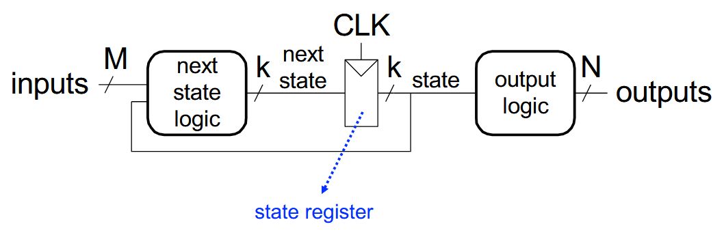
Front
ETH::2._Semester::DDCA::04a._Sequential_Logic_Design_II_&_Finite_State_Machines::02._Finite_State_Machines
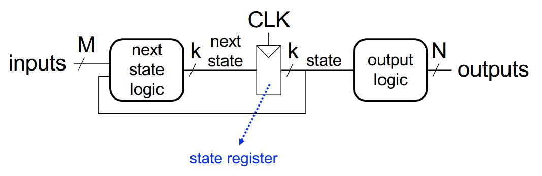
Each FSM consists of three separate parts:
next state logic state register output logic
Back
ETH::2._Semester::DDCA::04a._Sequential_Logic_Design_II_&_Finite_State_Machines::02._Finite_State_Machines
Each FSM consists of three separate parts:
next state logic state register output logic At the beginning of the clock cycle, next state is latched into the state register
Field-by-field Comparison
Field
Before
After
Text Each FSM consists of three separate parts:<br><ol><li>{{c1::next state logic}}</li><li>{{c2::state register}}</li><li>{{c3::output logic}}</li></ol>
Extra <img src="paste-f282a35cb1ef5e0d4f8f098548b2bdb621bdf0da.jpg"><br><br>At the beginning of the clock cycle, next state is latched into the state register
Tags:
ETH::2._Semester::DDCA::04a._Sequential_Logic_Design_II_&_Finite_State_Machines::02._Finite_State_Machines
Note 7: ETH::2. Semester::DDCA
Deck: ETH::2. Semester::DDCANote Type: Horvath ClozeGUID: P938wRh{~H
added
Previous
Note did not exist
New Note
Front
ETH::2._Semester::DDCA::04a._Sequential_Logic_Design_II_&_Finite_State_Machines::02._Finite_State_Machines
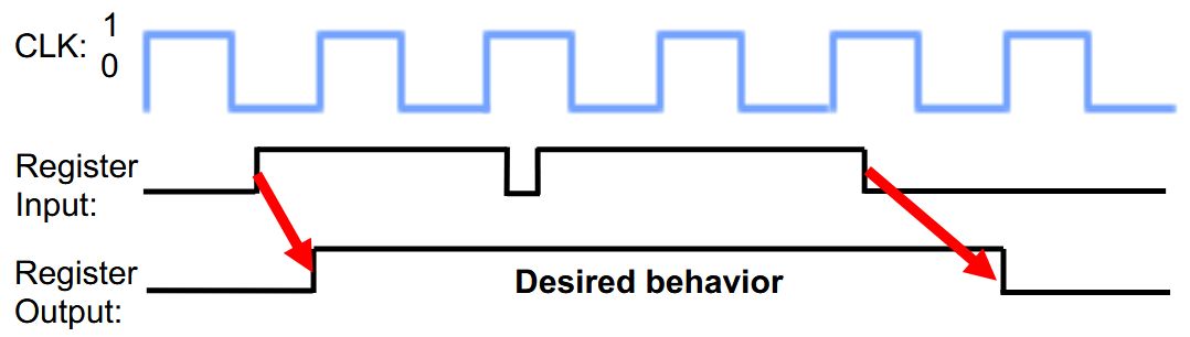
Which properties do we need to implement a state register?
We need to store data at the beginning of every clock cycle The data must be available during the entire clock cycle
Back
ETH::2._Semester::DDCA::04a._Sequential_Logic_Design_II_&_Finite_State_Machines::02._Finite_State_Machines
Which properties do we need to implement a state register?
We need to store data at the beginning of every clock cycle The data must be available during the entire clock cycle
Field-by-field Comparison
Field
Before
After
Text Which properties do we need to implement a state register?<br><ol><li>{{c1::We need to store data at the beginning of every clock cycle}}<br></li><li>{{c2::The data must be available during the entire clock cycle}}<br></li></ol>
Extra <img src="paste-d15605117cc9664c84a7753d40f0a3d09f3febbd.jpg"><br><img src="paste-f6afd0db6d1e758d9b809052a6b2ad201b0950b0.jpg">
Tags:
ETH::2._Semester::DDCA::04a._Sequential_Logic_Design_II_&_Finite_State_Machines::02._Finite_State_Machines
Note 8: ETH::2. Semester::DDCA
Deck: ETH::2. Semester::DDCANote Type: Horvath ClozeGUID: PMc1ViG{^J
added
Previous
Note did not exist
New Note
Front
ETH::2._Semester::DDCA::04a._Sequential_Logic_Design_II_&_Finite_State_Machines::01._Sequential_Logic_Circuits
Most modern computers are synchronous "machines"
Back
ETH::2._Semester::DDCA::04a._Sequential_Logic_Design_II_&_Finite_State_Machines::01._Sequential_Logic_Circuits
Most modern computers are synchronous "machines"
State transitions take place at fixed units of time (i.e., potentially delayed response to input, synchronized to an external signal).
Field-by-field Comparison
Field
Before
After
Text Most modern computers are {{c1::synchronous}} "machines"
Extra State transitions take place at fixed units of time (i.e., potentially delayed response to input, synchronized to an external signal).<br><br>Controlled in part by a clock, as we will see soon.
Tags:
ETH::2._Semester::DDCA::04a._Sequential_Logic_Design_II_&_Finite_State_Machines::01._Sequential_Logic_Circuits
Note 9: ETH::2. Semester::DDCA
Deck: ETH::2. Semester::DDCANote Type: Horvath OcclusioGUID: [,YWN{Lwu
added
Previous
Note did not exist
New Note
Front
ETH::2._Semester::DDCA::04a._Sequential_Logic_Design_II_&_Finite_State_Machines::05._Finite_State_Machine:_Schematic
Back
ETH::2._Semester::DDCA::04a._Sequential_Logic_Design_II_&_Finite_State_Machines::05._Finite_State_Machine:_Schematic
Field-by-field Comparison
Field
Before
After
Image <img src="paste-6a8326151aeedf40c81bab85eb67ee61a0bfdc28.jpg">
Header What is this?
Tags:
ETH::2._Semester::DDCA::04a._Sequential_Logic_Design_II_&_Finite_State_Machines::05._Finite_State_Machine:_Schematic
Note 10: ETH::2. Semester::DDCA
Deck: ETH::2. Semester::DDCANote Type: Horvath ClassicGUID: b]5EOR.;[y
added
Previous
Note did not exist
New Note
Front
ETH::2._Semester::DDCA::04a._Sequential_Logic_Design_II_&_Finite_State_Machines::02._Finite_State_Machines
What is a Finite State Machine (FSM)?
Back
ETH::2._Semester::DDCA::04a._Sequential_Logic_Design_II_&_Finite_State_Machines::02._Finite_State_Machines
What is a Finite State Machine (FSM)?
A discrete-time model of a stateful system.
Field-by-field Comparison
Field
Before
After
Front What is a Finite State Machine (FSM)?
Back A discrete-time model of a stateful system.<br><br>Each state represents a snapshot of the system at a given time.
Tags:
ETH::2._Semester::DDCA::04a._Sequential_Logic_Design_II_&_Finite_State_Machines::02._Finite_State_Machines
Note 11: ETH::2. Semester::DDCA
Deck: ETH::2. Semester::DDCANote Type: Horvath ClassicGUID: c.C#J,&->z
added
Previous
Note did not exist
New Note
Front
ETH::2._Semester::DDCA::04a._Sequential_Logic_Design_II_&_Finite_State_Machines::05._Finite_State_Machine:_Schematic
What is the non-greyed out part of the circuit?
Back
ETH::2._Semester::DDCA::04a._Sequential_Logic_Design_II_&_Finite_State_Machines::05._Finite_State_Machine:_Schematic
What is the non-greyed out part of the circuit?
Output logic and outputs.
Field-by-field Comparison
Field
Before
After
Front What is the non-greyed out part of the circuit?<br><br><img src="paste-e862550d817fcb452eefec1d1adda5fe368464f1.jpg">
Back Output logic and outputs.<br><br><img src="paste-cd6ef59f2ccfee5f7ab46a1cdc992280c12a7ba5.jpg">
Tags:
ETH::2._Semester::DDCA::04a._Sequential_Logic_Design_II_&_Finite_State_Machines::05._Finite_State_Machine:_Schematic
Note 12: ETH::2. Semester::DDCA
Deck: ETH::2. Semester::DDCANote Type: Horvath ClozeGUID: fj@3y5gt5P
added
Previous
Note did not exist
New Note
Front
ETH::2._Semester::DDCA::04a._Sequential_Logic_Design_II_&_Finite_State_Machines::01._Sequential_Logic_Circuits
The state of a system is a snapshot of all relevant elements of the system at the moment of the snapshot.
Back
ETH::2._Semester::DDCA::04a._Sequential_Logic_Design_II_&_Finite_State_Machines::01._Sequential_Logic_Circuits
The state of a system is a snapshot of all relevant elements of the system at the moment of the snapshot.
Field-by-field Comparison
Field
Before
After
Text The {{c1::state}} of a system is a snapshot of all relevant elements of the system at the moment of the snapshot.
Tags:
ETH::2._Semester::DDCA::04a._Sequential_Logic_Design_II_&_Finite_State_Machines::01._Sequential_Logic_Circuits
Note 13: ETH::2. Semester::DDCA
Deck: ETH::2. Semester::DDCANote Type: Horvath OcclusioGUID: g(oknS2XIO
added
Previous
Note did not exist
New Note
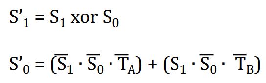
Front
ETH::2._Semester::DDCA::04a._Sequential_Logic_Design_II_&_Finite_State_Machines::03._Finite_State_Machine:_State_Transition_Table
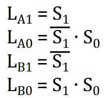
Determine the SOP of \(S_1'\) from this state transition table:
image-occlusion:rect:left=.1192:top=.7777:width=.5322:height=.0901:oi=1
Back
ETH::2._Semester::DDCA::04a._Sequential_Logic_Design_II_&_Finite_State_Machines::03._Finite_State_Machine:_State_Transition_Table
Determine the SOP of \(S_1'\) from this state transition table:
image-occlusion:rect:left=.1192:top=.7777:width=.5322:height=.0901:oi=1
Toggle Masks
Field-by-field Comparison
Field
Before
After
Occlusion {{c1::image-occlusion:rect:left=.1192:top=.7777:width=.5322:height=.0901:oi=1}}<br>
Image <img src="paste-2b0785e36a987370d617f3eeadb768dc3c9ce66d.jpg">
Header Determine the SOP of \(S_1'\) from this state transition table:
Tags:
ETH::2._Semester::DDCA::04a._Sequential_Logic_Design_II_&_Finite_State_Machines::03._Finite_State_Machine:_State_Transition_Table
Note 14: ETH::2. Semester::DDCA
Deck: ETH::2. Semester::DDCANote Type: Horvath ClozeGUID: g<38ETccf&
added
Previous
Note did not exist
New Note
Front
ETH::2._Semester::DDCA::04a._Sequential_Logic_Design_II_&_Finite_State_Machines::01._Sequential_Logic_Circuits
Combinational logic evaluates for the length of the clock cycle.
Back
ETH::2._Semester::DDCA::04a._Sequential_Logic_Design_II_&_Finite_State_Machines::01._Sequential_Logic_Circuits
Combinational logic evaluates for the length of the clock cycle.
Field-by-field Comparison
Field
Before
After
Text Combinational logic evaluates for the {{c1::length}} of the clock cycle.
Tags:
ETH::2._Semester::DDCA::04a._Sequential_Logic_Design_II_&_Finite_State_Machines::01._Sequential_Logic_Circuits
Note 15: ETH::2. Semester::DDCA
Deck: ETH::2. Semester::DDCANote Type: Horvath ClozeGUID: jgnr@Obi8f
added
Previous
Note did not exist
New Note
Front
ETH::2._Semester::DDCA::04a._Sequential_Logic_Design_II_&_Finite_State_Machines::02._Finite_State_Machines
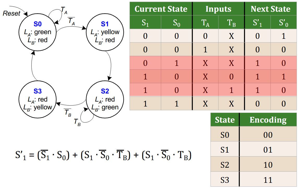
Two types of finite state machines differ in the output logic:
Moore FSM : outputs depend only on the current stateMealy FSM : outputs depend on the current state and the inputs
Back
ETH::2._Semester::DDCA::04a._Sequential_Logic_Design_II_&_Finite_State_Machines::02._Finite_State_Machines
Two types of finite state machines differ in the output logic:
Moore FSM : outputs depend only on the current stateMealy FSM : outputs depend on the current state and the inputs
Field-by-field Comparison
Field
Before
After
Text Two types of finite state machines differ in the output logic:<br><ol><li>{{c1::Moore FSM}}: outputs depend only on the current state</li><li>{{c2::Mealy FSM}}: outputs depend on the current state and the inputs</li></ol>
Extra <img src="paste-8c32ce33990f4253676703e6ef1745ff9f544c8e.jpg">
Tags:
ETH::2._Semester::DDCA::04a._Sequential_Logic_Design_II_&_Finite_State_Machines::02._Finite_State_Machines
Note 16: ETH::2. Semester::DDCA
Deck: ETH::2. Semester::DDCANote Type: Horvath ClozeGUID: km!Z
added
Previous
Note did not exist
New Note
Front
ETH::2._Semester::DDCA::04a._Sequential_Logic_Design_II_&_Finite_State_Machines::06._Finite_State_Machine:_State_Encoding
One-Hot Encoding :
Each bit encodes a different state
Uses num_states bits to represent the states
Exactly 1 bit is "hot" for a given state
Simplest design process – very automatableMinimizes next state logic , maximizes # flip-flops
Back
ETH::2._Semester::DDCA::04a._Sequential_Logic_Design_II_&_Finite_State_Machines::06._Finite_State_Machine:_State_Encoding
One-Hot Encoding :
Each bit encodes a different state
Uses num_states bits to represent the states
Exactly 1 bit is "hot" for a given state
Simplest design process – very automatableMinimizes next state logic , maximizes # flip-flops Example state encodings: 0001, 0010, 0100, 1000
Field-by-field Comparison
Field
Before
After
Text <div>{{c1::One-Hot Encoding}}<strong>:</strong></div>
<ul>
<li>Each bit {{c4::encodes a different state
<ul>
<li>Uses <em>num_states</em> bits to represent the states</li>
<li>Exactly 1 bit is "hot" for a given state</li></ul>}}</li>
<li><strong>Simplest design process</strong> – very automatable</li>
<li><strong>Minimizes</strong> {{c2::next state logic}}, <strong>maximizes</strong> {{c3::# flip-flops}}</li></ul>
Extra <em>Example state encodings:</em> 0001, 0010, 0100, 1000
Tags:
ETH::2._Semester::DDCA::04a._Sequential_Logic_Design_II_&_Finite_State_Machines::06._Finite_State_Machine:_State_Encoding
Note 17: ETH::2. Semester::DDCA
Deck: ETH::2. Semester::DDCANote Type: Horvath OcclusioGUID: l:)hd01;==
added
Previous
Note did not exist
New Note
Front
ETH::2._Semester::DDCA::04b._Introduction_to_the_Labs_and_FPGAs::06._More_about_FPGAs
What is this hidden component?
image-occlusion:rect:left=.3893:top=.0178:width=.4877:height=.0674:oi=1 image-occlusion:rect:left=.5552:top=.3107:width=.4354:height=.1021:oi=1
Back
ETH::2._Semester::DDCA::04b._Introduction_to_the_Labs_and_FPGAs::06._More_about_FPGAs
What is this hidden component?
image-occlusion:rect:left=.3893:top=.0178:width=.4877:height=.0674:oi=1 image-occlusion:rect:left=.5552:top=.3107:width=.4354:height=.1021:oi=1
Toggle Masks
Field-by-field Comparison
Field
Before
After
Occlusion {{c1::image-occlusion:rect:left=.3893:top=.0178:width=.4877:height=.0674:oi=1}}<br>{{c2::image-occlusion:rect:left=.5552:top=.3107:width=.4354:height=.1021:oi=1}}<br>
Image <img src="paste-bc35d0ae17174e4109a0bc070e1da9b4d468886b.jpg">
Header What is this hidden component?
Tags:
ETH::2._Semester::DDCA::04b._Introduction_to_the_Labs_and_FPGAs::06._More_about_FPGAs
Note 18: ETH::2. Semester::DDCA
Deck: ETH::2. Semester::DDCANote Type: Horvath ClassicGUID: nZ9{K+v5e:
added
Previous
Note did not exist
New Note
Front
ETH::2._Semester::DDCA::04a._Sequential_Logic_Design_II_&_Finite_State_Machines::05._Finite_State_Machine:_Schematic
What is this?
Back
ETH::2._Semester::DDCA::04a._Sequential_Logic_Design_II_&_Finite_State_Machines::05._Finite_State_Machine:_Schematic
What is this?
A state register.
Field-by-field Comparison
Field
Before
After
Front What is this?<br><br><img src="paste-4acc4c494556bcdc7cbaf9afc6e9b6e94385de83.jpg">
Back A state register.
Tags:
ETH::2._Semester::DDCA::04a._Sequential_Logic_Design_II_&_Finite_State_Machines::05._Finite_State_Machine:_Schematic
Note 19: ETH::2. Semester::DDCA
Deck: ETH::2. Semester::DDCANote Type: Horvath ClozeGUID: oO*YyBr@a8
added
Previous
Note did not exist
New Note
Front
ETH::2._Semester::DDCA::04a._Sequential_Logic_Design_II_&_Finite_State_Machines::02._Finite_State_Machines
We can use D Flip-Flops to implement the state register.
Back
ETH::2._Semester::DDCA::04a._Sequential_Logic_Design_II_&_Finite_State_Machines::02._Finite_State_Machines
We can use D Flip-Flops to implement the state register.
Field-by-field Comparison
Field
Before
After
Text We can use {{c1::D Flip-Flops}} to implement the state register.
Extra <img src="paste-2f7dcb7191f560d4f7710228edba5ec2380729ab.jpg">
Tags:
ETH::2._Semester::DDCA::04a._Sequential_Logic_Design_II_&_Finite_State_Machines::02._Finite_State_Machines
Note 20: ETH::2. Semester::DDCA
Deck: ETH::2. Semester::DDCANote Type: Horvath ClozeGUID: p}!>Qc
added
Previous
Note did not exist
New Note
Front
ETH::2._Semester::DDCA::04b._Introduction_to_the_Labs_and_FPGAs::03._What_is_an_FPGA
A FPGA is a software-reconfigurable hardware substrate .
Back
ETH::2._Semester::DDCA::04b._Introduction_to_the_Labs_and_FPGAs::03._What_is_an_FPGA
A FPGA is a software-reconfigurable hardware substrate .
Reconfigurable functions Reconfigurable interconnection of functions Reconfigurable input/output (IO)
Field-by-field Comparison
Field
Before
After
Text A FPGA is a {{c1::software-reconfigurable hardware substrate}}.
Extra <ul><li>Reconfigurable functions</li><li>Reconfigurable interconnection of functions</li><li>Reconfigurable input/output (IO)</li></ul>
Tags:
ETH::2._Semester::DDCA::04b._Introduction_to_the_Labs_and_FPGAs::03._What_is_an_FPGA
Note 21: ETH::2. Semester::DDCA
Deck: ETH::2. Semester::DDCANote Type: Horvath ClozeGUID: rnH{-|yj$G
added
Previous
Note did not exist
New Note
Front
ETH::2._Semester::DDCA::04a._Sequential_Logic_Design_II_&_Finite_State_Machines::01._Sequential_Logic_Circuits
A clock synchronizes state changes across many sequential circuit elements.
Back
ETH::2._Semester::DDCA::04a._Sequential_Logic_Design_II_&_Finite_State_Machines::01._Sequential_Logic_Circuits
A clock synchronizes state changes across many sequential circuit elements.
Field-by-field Comparison
Field
Before
After
Text A clock {{c1::synchronizes state changes}} across many sequential circuit elements.
Tags:
ETH::2._Semester::DDCA::04a._Sequential_Logic_Design_II_&_Finite_State_Machines::01._Sequential_Logic_Circuits
Note 22: ETH::2. Semester::DDCA
Deck: ETH::2. Semester::DDCANote Type: Horvath ClassicGUID: r}x`DbeK*8
added
Previous
Note did not exist
New Note
Front
ETH::2._Semester::DDCA::04b._Introduction_to_the_Labs_and_FPGAs::06._More_about_FPGAs
What are the two main building blocks of FPGAs?
Back
ETH::2._Semester::DDCA::04b._Introduction_to_the_Labs_and_FPGAs::06._More_about_FPGAs
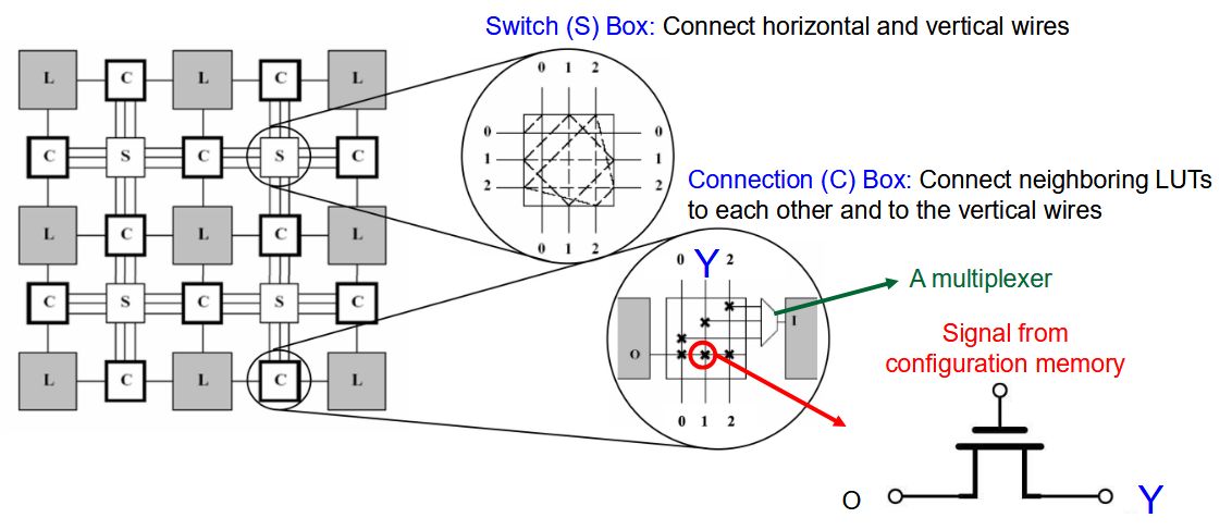
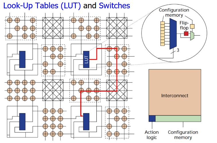
What are the two main building blocks of FPGAs?
Look-Up Tables (LUT) and Switches.
Field-by-field Comparison
Field
Before
After
Front What are the two main building blocks of FPGAs?
Back Look-Up Tables (LUT) and Switches.<br><br><img src="paste-cee6c807e9f899a8a1405b26996492bb8e767dc2.jpg">
Tags:
ETH::2._Semester::DDCA::04b._Introduction_to_the_Labs_and_FPGAs::06._More_about_FPGAs
Note 23: ETH::2. Semester::DDCA
Deck: ETH::2. Semester::DDCANote Type: Horvath ClassicGUID: s&4,le+tM#
added
Previous
Note did not exist
New Note
Front
ETH::2._Semester::DDCA::04a._Sequential_Logic_Design_II_&_Finite_State_Machines::05._Finite_State_Machine:_Schematic
What is the non-greyed out part of the circuit?
Back
ETH::2._Semester::DDCA::04a._Sequential_Logic_Design_II_&_Finite_State_Machines::05._Finite_State_Machine:_Schematic
What is the non-greyed out part of the circuit?
Inputs and next state logic.
Field-by-field Comparison
Field
Before
After
Front What is the non-greyed out part of the circuit?<br><br><img src="paste-85e71c9bf7ed1a2185c5aced59218c7ccf5c67e2.jpg">
Back Inputs and next state logic.<br><br><img src="paste-b7f3dd92498680d0dc3a9552c5869110b8305375.jpg">
Tags:
ETH::2._Semester::DDCA::04a._Sequential_Logic_Design_II_&_Finite_State_Machines::05._Finite_State_Machine:_Schematic
Note 24: ETH::2. Semester::DDCA
Deck: ETH::2. Semester::DDCANote Type: Horvath ClassicGUID: sQP[*On3|~
added
Previous
Note did not exist
New Note
Front
ETH::2._Semester::DDCA::04a._Sequential_Logic_Design_II_&_Finite_State_Machines::02._Finite_State_Machines
Which types of circuits are the three parts of a FSM?
Back
ETH::2._Semester::DDCA::04a._Sequential_Logic_Design_II_&_Finite_State_Machines::02._Finite_State_Machines
Which types of circuits are the three parts of a FSM?
Sequential Circuits: State register(s)
Combinatorial Circuits: Next state logic, Output logic
Field-by-field Comparison
Field
Before
After
Front Which types of circuits are the three parts of a FSM?
Back Sequential Circuits: State register(s)<br>Combinatorial Circuits: Next state logic, Output logic<br><br><img src="paste-e4af3b21078ddee189e7c5399eb242bb5d90fd10.jpg">
Tags:
ETH::2._Semester::DDCA::04a._Sequential_Logic_Design_II_&_Finite_State_Machines::02._Finite_State_Machines
Note 25: ETH::2. Semester::DDCA
Deck: ETH::2. Semester::DDCANote Type: Horvath ClozeGUID: sdsi1t>JHJ
added
Previous
Note did not exist
New Note
Front
ETH::2._Semester::DDCA::04a._Sequential_Logic_Design_II_&_Finite_State_Machines::01._Sequential_Logic_Circuits
A clock cycle should be chosen to accommodate the maximum combinational circuit delay .
Back
ETH::2._Semester::DDCA::04a._Sequential_Logic_Design_II_&_Finite_State_Machines::01._Sequential_Logic_Circuits
A clock cycle should be chosen to accommodate the maximum combinational circuit delay .
Field-by-field Comparison
Field
Before
After
Text A clock cycle should be chosen to accommodate {{c1::the maximum combinational circuit delay}}.
Tags:
ETH::2._Semester::DDCA::04a._Sequential_Logic_Design_II_&_Finite_State_Machines::01._Sequential_Logic_Circuits
Note 26: ETH::2. Semester::DDCA
Deck: ETH::2. Semester::DDCANote Type: Horvath ClassicGUID: tB@;-gL*Hb
added
Previous
Note did not exist
New Note
Front
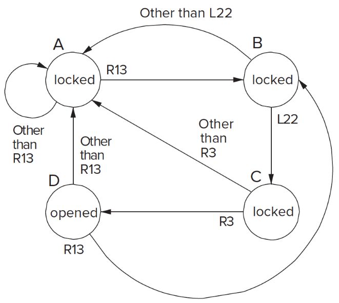
ETH::2._Semester::DDCA::04a._Sequential_Logic_Design_II_&_Finite_State_Machines::01._Sequential_Logic_Circuits
What is this?
Back
ETH::2._Semester::DDCA::04a._Sequential_Logic_Design_II_&_Finite_State_Machines::01._Sequential_Logic_Circuits
What is this?
State diagram of a sequential lock.
Field-by-field Comparison
Field
Before
After
Front What is this?<br><br><img src="paste-8aec0ef28faf022ade42db3b79a541216adc891c.jpg">
Back State diagram of a sequential lock.
Tags:
ETH::2._Semester::DDCA::04a._Sequential_Logic_Design_II_&_Finite_State_Machines::01._Sequential_Logic_Circuits
Note 27: ETH::2. Semester::DDCA
Deck: ETH::2. Semester::DDCANote Type: Horvath ClozeGUID: tqA%.|md]&
added
Previous
Note did not exist
New Note
Front
ETH::2._Semester::DDCA::04a._Sequential_Logic_Design_II_&_Finite_State_Machines::06._Finite_State_Machine:_State_Encoding
Output Encoding:
Outputs are directly accessible in the state encoding For the traffic light example, since we have 3 outputs (light color), encode state with 3 bits , where each bit represents a color Minimizes output logic Only works for Moore Machines (output function of state)
Back
ETH::2._Semester::DDCA::04a._Sequential_Logic_Design_II_&_Finite_State_Machines::06._Finite_State_Machine:_State_Encoding
Output Encoding:
Outputs are directly accessible in the state encoding For the traffic light example, since we have 3 outputs (light color), encode state with 3 bits , where each bit represents a color Minimizes output logic Only works for Moore Machines (output function of state) Example states: 001, 010, 100, 110
Bit₀ encodes green light output Bit₁ encodes yellow light output Bit₂ encodes red light output
Field-by-field Comparison
Field
Before
After
Text <div><div>{{c1::Output}}<strong>Encoding:</strong></div>
<ul>
<li>Outputs are <strong>directly accessible</strong> in the state encoding</li><li>For the traffic light example, since we have <strong>3 outputs</strong> (light color), encode state with <strong>3 bits</strong>, where each bit represents a color</li><li><strong>Minimizes</strong> {{c2::output logic}}</li><li>Only works for Moore Machines (output function of state)</li></ul></div><br>
Extra <em>Example states:</em> 001, 010, 100, 110<br><ul><li>Bit₀ encodes <strong>green</strong> light output</li><li>Bit₁ encodes <strong>yellow</strong> light output</li><li>Bit₂ encodes <strong>red</strong> light output</li></ul>
Tags:
ETH::2._Semester::DDCA::04a._Sequential_Logic_Design_II_&_Finite_State_Machines::06._Finite_State_Machine:_State_Encoding
Note 28: ETH::2. Semester::DDCA
Deck: ETH::2. Semester::DDCANote Type: Horvath ClozeGUID: u_>,$|fP)p
added
Previous
Note did not exist
New Note
Front
ETH::2._Semester::DDCA::04a._Sequential_Logic_Design_II_&_Finite_State_Machines::06._Finite_State_Machine:_State_Encoding
Binary Encoding (Full Encoding) :
Use the minimum possible number of bits
Use log₂(num_states) bits to represent the states
Minimizes # flip-flops, but not necessarily output logic or next state logic
Back
ETH::2._Semester::DDCA::04a._Sequential_Logic_Design_II_&_Finite_State_Machines::06._Finite_State_Machine:_State_Encoding
Binary Encoding (Full Encoding) :
Use the minimum possible number of bits
Use log₂(num_states) bits to represent the states
Minimizes # flip-flops, but not necessarily output logic or next state logic Example state encodings: 00, 01, 10, 11
Field-by-field Comparison
Field
Before
After
Text <div>{{c1::Binary Encoding (Full Encoding)}}<strong>:</strong></div>
<ul>
<li>Use {{c3::the minimum possible number of}} bits
<ul>
<li>{{c3::Use <em>log₂(num_states)</em> bits to represent the states}}<br></li></ul></li>
<li><strong>Minimizes</strong> {{c2::# flip-flops, but not necessarily output logic or next state logic}}</li></ul>
Extra <em>Example state encodings:</em> 00, 01, 10, 11
Tags:
ETH::2._Semester::DDCA::04a._Sequential_Logic_Design_II_&_Finite_State_Machines::06._Finite_State_Machine:_State_Encoding
Note 29: ETH::2. Semester::DDCA
Deck: ETH::2. Semester::DDCANote Type: Horvath ClassicGUID: uw+8DkpUY4
added
Previous
Note did not exist
New Note
Front
ETH::2._Semester::DDCA::04a._Sequential_Logic_Design_II_&_Finite_State_Machines::02._Finite_State_Machines
What is this?
Back
ETH::2._Semester::DDCA::04a._Sequential_Logic_Design_II_&_Finite_State_Machines::02._Finite_State_Machines
What is this?
A D Flip-Flop.
Field-by-field Comparison
Field
Before
After
Front What is this?<br><br><img src="paste-3786bddf98da046a8599b4333c56fc1317667876.jpg">
Back A D Flip-Flop.<br><br>At the rising edge of clock (clock going from 0\(\rightarrow\)1), Q gets assigned D.<br>At all other times, Q is unchanged.
Tags:
ETH::2._Semester::DDCA::04a._Sequential_Logic_Design_II_&_Finite_State_Machines::02._Finite_State_Machines
Note 30: ETH::2. Semester::DDCA
Deck: ETH::2. Semester::DDCANote Type: Horvath ClassicGUID: v}t`qx*Ktt
added
Previous
Note did not exist
New Note
Front
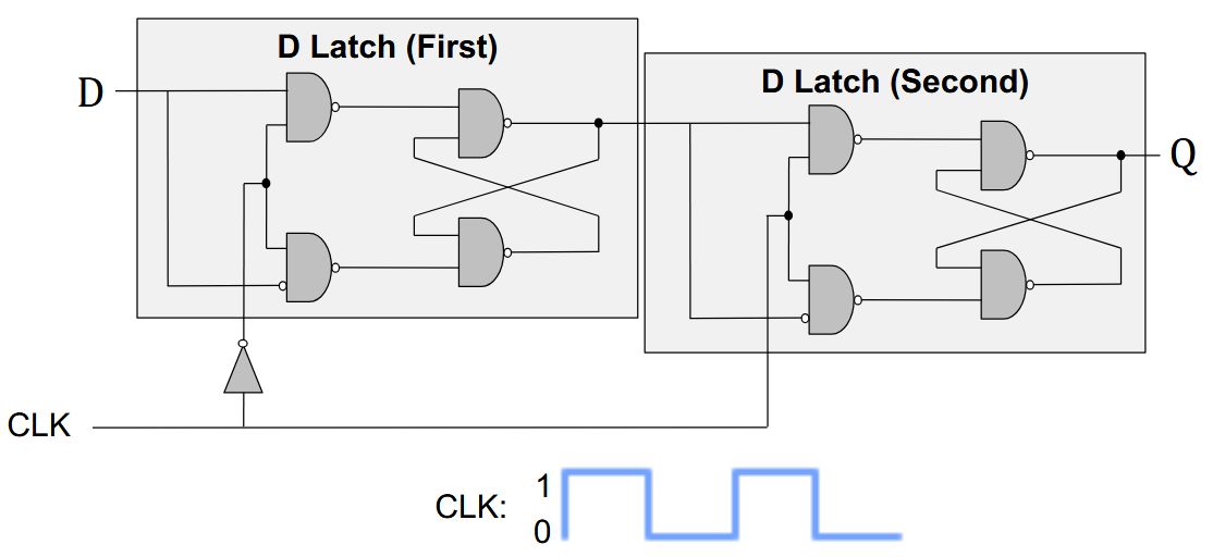
ETH::2._Semester::DDCA::04a._Sequential_Logic_Design_II_&_Finite_State_Machines::02._Finite_State_Machines
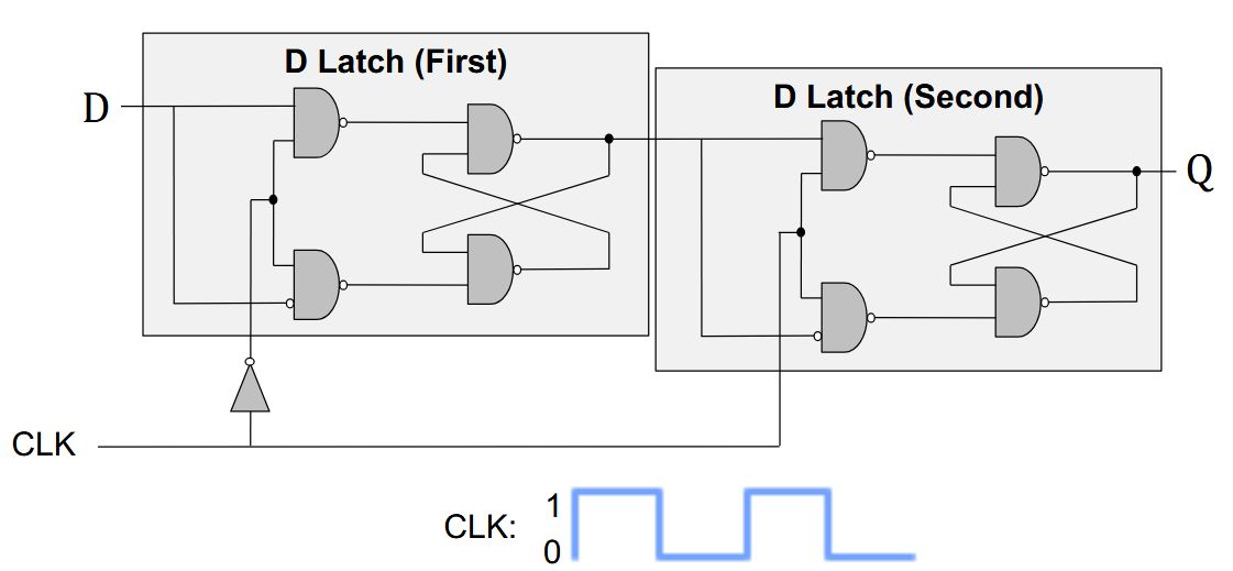
How can we use D Latches to implement a FSM?
Back
ETH::2._Semester::DDCA::04a._Sequential_Logic_Design_II_&_Finite_State_Machines::02._Finite_State_Machines
How can we use D Latches to implement a FSM?
We use a D Flip-Flop
When the clock is low, 1st latch propagates D to the input of the 2nd (Q unchanged).
Only when the clock is high, 2nd latch latches D (Q stores D).
At the rising edge of clock (clock going from 0\(\rightarrow\)1), Q gets assigned D.
Field-by-field Comparison
Field
Before
After
Front How can we use D Latches to implement a FSM?
Back We use a D Flip-Flop<br><img src="paste-cc73c8e859236da274b023d8fb58b5b1d90451f3.jpg"><br><br>When the clock is low, 1st latch propagates D to the input of the 2nd (Q unchanged).<br><br>Only when the clock is high, 2nd latch latches D (Q stores D).<br>At the rising edge of clock (clock going from 0\(\rightarrow\)1), Q gets assigned D.
Tags:
ETH::2._Semester::DDCA::04a._Sequential_Logic_Design_II_&_Finite_State_Machines::02._Finite_State_Machines
Note 31: ETH::2. Semester::DDCA
Deck: ETH::2. Semester::DDCANote Type: Horvath ClozeGUID: x!EU,iyr5{
added
Previous
Note did not exist
New Note
Front
ETH::2._Semester::DDCA::04a._Sequential_Logic_Design_II_&_Finite_State_Machines::02._Finite_State_Machines
A FSM consists of these elements:
A finite number of states A finite number of external inputs A finite number of external outputs An explicit specification of all state transitions An explicit specification of what determines each external output value
Back
ETH::2._Semester::DDCA::04a._Sequential_Logic_Design_II_&_Finite_State_Machines::02._Finite_State_Machines
A FSM consists of these elements:
A finite number of states A finite number of external inputs A finite number of external outputs An explicit specification of all state transitions An explicit specification of what determines each external output value State: snapshot of all relevant elements of the system at the time of the snapshot
Field-by-field Comparison
Field
Before
After
Text A FSM consists of these elements:<br><ol><li>{{c1::A finite number of states}}</li><li>{{c2::A finite number of external inputs}}<br></li><li>{{c2::A finite number of external outputs}}</li><li>{{c3::An explicit specification of all state transitions}}</li><li>{{c4::An explicit specification of what determines each external output value}}<br></li></ol>
Extra State: snapshot of all relevant elements of the system at the time of the snapshot
Tags:
ETH::2._Semester::DDCA::04a._Sequential_Logic_Design_II_&_Finite_State_Machines::02._Finite_State_Machines
Note 32: ETH::2. Semester::DDCA
Deck: ETH::2. Semester::DDCANote Type: Horvath OcclusioGUID: y!>GF#oDFU
added
Previous
Note did not exist
New Note
Front
ETH::2._Semester::DDCA::04a._Sequential_Logic_Design_II_&_Finite_State_Machines::04._Finite_State_Machine:_Output_Table
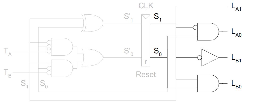
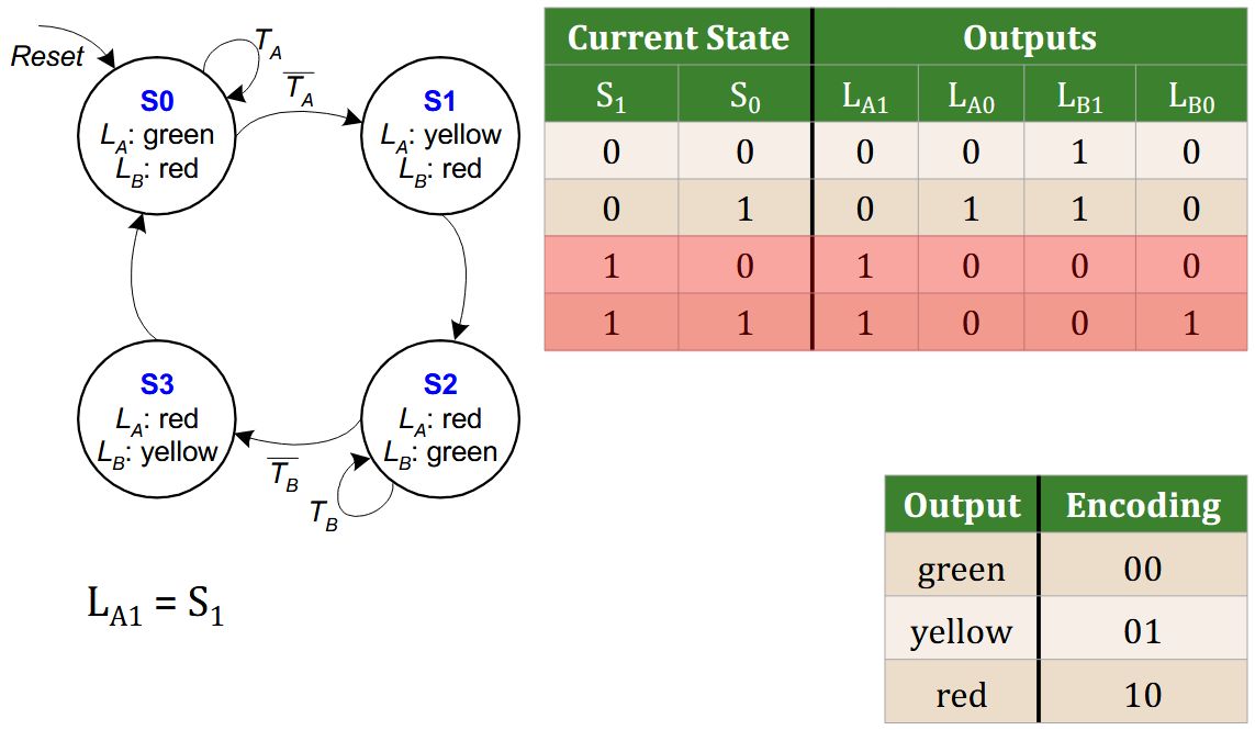
Determine the SOP of \(L_{A1}\) from this output table:
image-occlusion:rect:left=.1448:top=.7889:width=.1955:height=.0794:oi=1
Back
ETH::2._Semester::DDCA::04a._Sequential_Logic_Design_II_&_Finite_State_Machines::04._Finite_State_Machine:_Output_Table
Determine the SOP of \(L_{A1}\) from this output table:
image-occlusion:rect:left=.1448:top=.7889:width=.1955:height=.0794:oi=1
Toggle Masks
Field-by-field Comparison
Field
Before
After
Occlusion {{c1::image-occlusion:rect:left=.1448:top=.7889:width=.1955:height=.0794:oi=1}}<br>
Image <img src="paste-2104652c4307f2325008cef16a8a906d2b837817.jpg">
Header Determine the SOP of \(L_{A1}\) from this output table:
Tags:
ETH::2._Semester::DDCA::04a._Sequential_Logic_Design_II_&_Finite_State_Machines::04._Finite_State_Machine:_Output_Table
Note 33: ETH::2. Semester::DDCA
Deck: ETH::2. Semester::DDCANote Type: Horvath ClassicGUID: y2>qnHc%Pf
added
Previous
Note did not exist
New Note
Front
ETH::2._Semester::DDCA::04a._Sequential_Logic_Design_II_&_Finite_State_Machines::02._Finite_State_Machines
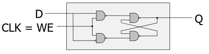
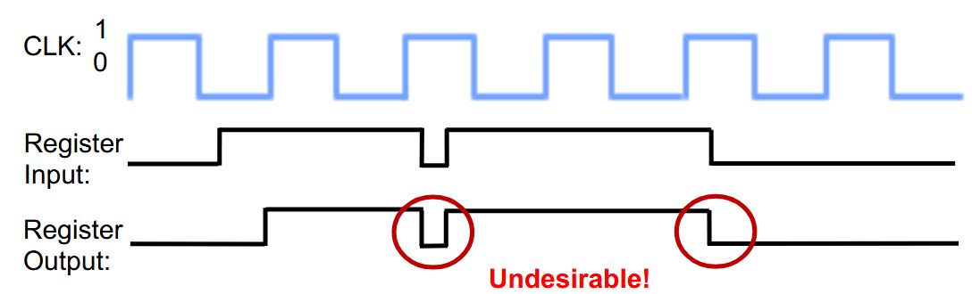
Why can't we simply wire a clock to WE of a D Latch to implement a FSM?
Back
ETH::2._Semester::DDCA::04a._Sequential_Logic_Design_II_&_Finite_State_Machines::02._Finite_State_Machines
Why can't we simply wire a clock to WE of a D Latch to implement a FSM?
Whenever the clock is high, the latch propagates D to Q.
The latch is "transparent".
Field-by-field Comparison
Field
Before
After
Front Why can't we simply wire a clock to WE of a D Latch to implement a FSM?<br><br><img src="paste-efb7af3e85cc5c79a9c81bbd59733d3e8ab3a4d2.jpg">
Back Whenever the clock is high, the latch propagates D to Q.<br>The latch is "transparent".<br><br><img src="paste-4414073a5709ca8e5710a64953abd1a4140c689c.jpg">
Tags:
ETH::2._Semester::DDCA::04a._Sequential_Logic_Design_II_&_Finite_State_Machines::02._Finite_State_Machines
Note 34: ETH::2. Semester::DDCA
Deck: ETH::2. Semester::DDCANote Type: Horvath ClozeGUID: zh6Oh%kTi<
added
Previous
Note did not exist
New Note
Front
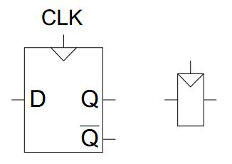
ETH::2._Semester::DDCA::04a._Sequential_Logic_Design_II_&_Finite_State_Machines::02._Finite_State_Machines
How does a rising-clock-edge triggered Flip-Flop work?
Two inputs: CLK, D
Function:
The flip-flop "samples" D on the rising edge of CLK (positive edge) When CLK rises from 0 to 1, D passes through to Q Otherwise, Q holds its previous value Q changes only on the rising edge of CLK
Back
ETH::2._Semester::DDCA::04a._Sequential_Logic_Design_II_&_Finite_State_Machines::02._Finite_State_Machines
How does a rising-clock-edge triggered Flip-Flop work?
Two inputs: CLK, D
Function:
The flip-flop "samples" D on the rising edge of CLK (positive edge) When CLK rises from 0 to 1, D passes through to Q Otherwise, Q holds its previous value Q changes only on the rising edge of CLK
Field-by-field Comparison
Field
Before
After
Text How does a rising-clock-edge triggered Flip-Flop work?<br><br><img src="paste-967b8524a938dc72302521297e9b9c8e8f17928c.jpg"><br><br>Two inputs: CLK, D<br><br>Function:<br><ol><li>The flip-flop "samples" D on {{c1::the rising edge of CLK (positive edge)}}</li><li>When CLK rises from 0 to 1, D {{c2::passes through to Q}}</li><li>Otherwise, {{c2::Q holds its previous value}}</li><li>Q changes only on {{c3::the rising edge of CLK}}</li></ol>
Tags:
ETH::2._Semester::DDCA::04a._Sequential_Logic_Design_II_&_Finite_State_Machines::02._Finite_State_Machines