Note 1: ETH::2. Semester::DDCA
Deck: ETH::2. Semester::DDCANote Type: Horvath ClozeGUID: B8FT@NiVSO
added
Previous
Note did not exist
New Note
Front
ETH::2._Semester::DDCA::03._Combinational_Logic_II_and_Sequential_Logic::11._Basic_Element:_Cross-Coupled_Inverters
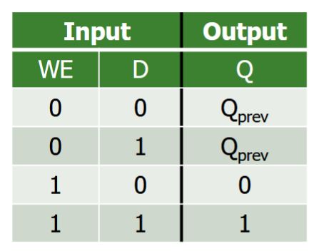
Pros and cons of Dynamic RAM (DRAM)
Cheap (one bit costs only one transistor plus one capacitor) Slower, reading destroys content (refresh), needs special process for manufacturing
Back
ETH::2._Semester::DDCA::03._Combinational_Logic_II_and_Sequential_Logic::11._Basic_Element:_Cross-Coupled_Inverters
Pros and cons of Dynamic RAM (DRAM)
Cheap (one bit costs only one transistor plus one capacitor) Slower, reading destroys content (refresh), needs special process for manufacturing
Field-by-field Comparison
Field
Before
After
Text Pros and cons of Dynamic RAM (DRAM)<ul><li>{{c1::Cheap (one bit costs only one transistor plus one capacitor)}}</li><li>{{c2::Slower, reading destroys content (refresh), needs special process for manufacturing}}</li></ul>
Tags:
ETH::2._Semester::DDCA::03._Combinational_Logic_II_and_Sequential_Logic::11._Basic_Element:_Cross-Coupled_Inverters
Note 2: ETH::2. Semester::DDCA
Deck: ETH::2. Semester::DDCANote Type: Horvath ClassicGUID: D[owgbdJ
added
Previous
Note did not exist
New Note
Front
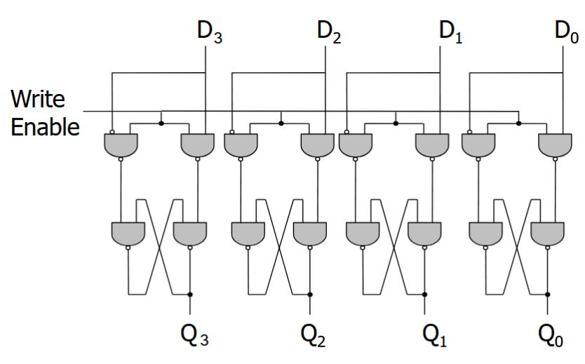
ETH::2._Semester::DDCA::03._Combinational_Logic_II_and_Sequential_Logic::14._Register
What is this?
Back
ETH::2._Semester::DDCA::03._Combinational_Logic_II_and_Sequential_Logic::14._Register
What is this?
Here we have a register, or a structure that stores more than one bit and can be read from and written to.
Field-by-field Comparison
Field
Before
After
Front What is this?<br><br><img src="paste-be78c3f8e3954dfc7609bb2b8a3310972620f5c8.jpg">
Back Here we have a register, or a structure that stores more than one bit and can be read from and written to.<br><br>Note that there is a single WE signal for all latches for simultaneous writes.<br><br>This register holds 4 bits, and its data is referenced as Q[3:0].
Tags:
ETH::2._Semester::DDCA::03._Combinational_Logic_II_and_Sequential_Logic::14._Register
Note 3: ETH::2. Semester::DDCA
Deck: ETH::2. Semester::DDCANote Type: Horvath ClozeGUID: GT1cT:#V..
added
Previous
Note did not exist
New Note
Front
ETH::2._Semester::DDCA::03._Combinational_Logic_II_and_Sequential_Logic::11._Basic_Element:_Cross-Coupled_Inverters
Pros and cons of Static RAM (SRAM)
Relatively fast Expensive (one bit costs 6+ transistors)
Back
ETH::2._Semester::DDCA::03._Combinational_Logic_II_and_Sequential_Logic::11._Basic_Element:_Cross-Coupled_Inverters
Pros and cons of Static RAM (SRAM)
Relatively fast Expensive (one bit costs 6+ transistors)
Field-by-field Comparison
Field
Before
After
Text Pros and cons of Static RAM (SRAM)<br><ul><li>{{c1::Relatively fast}}</li><li>{{c2::Expensive (one bit costs 6+ transistors)}}</li></ul>
Tags:
ETH::2._Semester::DDCA::03._Combinational_Logic_II_and_Sequential_Logic::11._Basic_Element:_Cross-Coupled_Inverters
Note 4: ETH::2. Semester::DDCA
Deck: ETH::2. Semester::DDCANote Type: Horvath ClozeGUID: GW`le=_OwA
added
Previous
Note did not exist
New Note
Front
ETH::2._Semester::DDCA::03._Combinational_Logic_II_and_Sequential_Logic::3._Logical_Completeness
Any logic function we wish to implement could be accomplished with a PLA.
Back
ETH::2._Semester::DDCA::03._Combinational_Logic_II_and_Sequential_Logic::3._Logical_Completeness
Any logic function we wish to implement could be accomplished with a PLA.
PLA consists of only AND gates, OR gates, and inverters.
Field-by-field Comparison
Field
Before
After
Text {{c1::Any::Quantity?}} logic function we wish to implement could be accomplished with a PLA.
Extra PLA consists of only AND gates, OR gates, and inverters.<br><br>We just have to program connections based on SOP of the intended logic function.
Tags:
ETH::2._Semester::DDCA::03._Combinational_Logic_II_and_Sequential_Logic::3._Logical_Completeness
Note 5: ETH::2. Semester::DDCA
Deck: ETH::2. Semester::DDCANote Type: Horvath OcclusioGUID: HIk47Ngez+
added
Previous
Note did not exist
New Note
Front
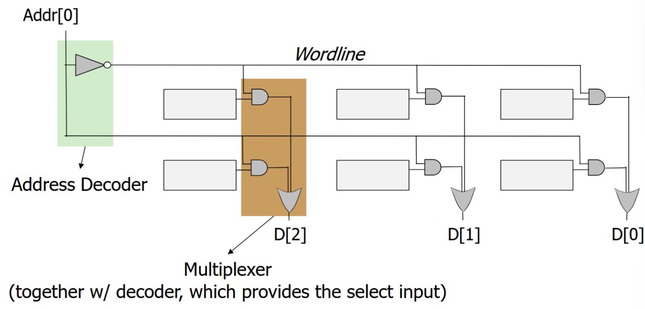
ETH::2._Semester::DDCA::03._Combinational_Logic_II_and_Sequential_Logic::15._Memory
How can we select an address to read?
image-occlusion:rect:left=.0089:top=.5477:width=.2313:height=.092 image-occlusion:rect:left=.0059:top=.8424:width=.7046:height=.1459
Back
ETH::2._Semester::DDCA::03._Combinational_Logic_II_and_Sequential_Logic::15._Memory
How can we select an address to read?
image-occlusion:rect:left=.0089:top=.5477:width=.2313:height=.092 image-occlusion:rect:left=.0059:top=.8424:width=.7046:height=.1459
Toggle Masks
Field-by-field Comparison
Field
Before
After
Occlusion {{c1::image-occlusion:rect:left=.0089:top=.5477:width=.2313:height=.092}}<br>{{c2::image-occlusion:rect:left=.0059:top=.8424:width=.7046:height=.1459}}<br>
Image <img src="paste-cd3e2c310623833536d291253844967607e468c8.jpg">
Header How can we select an address to read?
Tags:
ETH::2._Semester::DDCA::03._Combinational_Logic_II_and_Sequential_Logic::15._Memory
Note 6: ETH::2. Semester::DDCA
Deck: ETH::2. Semester::DDCANote Type: Horvath ClozeGUID: IjnwO_e62-
added
Previous
Note did not exist
New Note
Front
ETH::2._Semester::DDCA::03._Combinational_Logic_II_and_Sequential_Logic::11._Basic_Element:_Cross-Coupled_Inverters
Pros and Cons of Latches and Flip-Flops:
Very fast, parallel access Very expensive (one bit costs tens of transistors)
Back
ETH::2._Semester::DDCA::03._Combinational_Logic_II_and_Sequential_Logic::11._Basic_Element:_Cross-Coupled_Inverters
Pros and Cons of Latches and Flip-Flops:
Very fast, parallel access Very expensive (one bit costs tens of transistors)
Field-by-field Comparison
Field
Before
After
Text Pros and Cons of Latches and Flip-Flops:<br><ul><li>{{c1::Very fast, parallel access}}</li><li>{{c2::Very expensive (one bit costs tens of transistors)}}</li></ul>
Tags:
ETH::2._Semester::DDCA::03._Combinational_Logic_II_and_Sequential_Logic::11._Basic_Element:_Cross-Coupled_Inverters
Note 7: ETH::2. Semester::DDCA
Deck: ETH::2. Semester::DDCANote Type: Horvath ClassicGUID: J!Fb=eJD*B
added
Previous
Note did not exist
New Note
Front
ETH::2._Semester::DDCA::03._Combinational_Logic_II_and_Sequential_Logic::15._Memory
Addressability?
Back
ETH::2._Semester::DDCA::03._Combinational_Logic_II_and_Sequential_Logic::15._Memory
Addressability?
3-bits
Field-by-field Comparison
Field
Before
After
Front Addressability?<br><br><img src="paste-adeed554f607d7f9c2ae3a806f83b02c89cef624.jpg">
Back 3-bits
Tags:
ETH::2._Semester::DDCA::03._Combinational_Logic_II_and_Sequential_Logic::15._Memory
Note 8: ETH::2. Semester::DDCA
Deck: ETH::2. Semester::DDCANote Type: Horvath ClassicGUID: J}Cp1R>RJL
added
Previous
Note did not exist
New Note
Front
ETH::2._Semester::DDCA::03._Combinational_Logic_II_and_Sequential_Logic::16._Aside:_Implementing_Logic_Functions_Using_Memory
What is this functionally?
Back
ETH::2._Semester::DDCA::03._Combinational_Logic_II_and_Sequential_Logic::16._Aside:_Implementing_Logic_Functions_Using_Memory
What is this functionally?
A memory-bassed lookup table.
Field-by-field Comparison
Field
Before
After
Front What is this functionally?<br><br><img src="paste-da1444290ceb76a444f3cae190bb00d91cbf15ff.jpg">
Back A memory-bassed lookup table.
Tags:
ETH::2._Semester::DDCA::03._Combinational_Logic_II_and_Sequential_Logic::16._Aside:_Implementing_Logic_Functions_Using_Memory
Note 9: ETH::2. Semester::DDCA
Deck: ETH::2. Semester::DDCANote Type: Horvath ClassicGUID: MZTQ<6vlZH
added
Previous
Note did not exist
New Note
Front
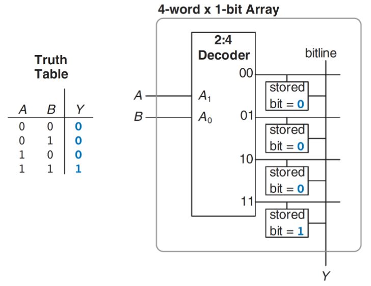
ETH::2._Semester::DDCA::03._Combinational_Logic_II_and_Sequential_Logic::7._Logic_Simplification_using_Boolean_Algebra_Rules
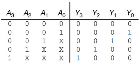
What do the X's here mean?
Back
ETH::2._Semester::DDCA::03._Combinational_Logic_II_and_Sequential_Logic::7._Logic_Simplification_using_Boolean_Algebra_Rules
What do the X's here mean?
X (Don't Care) means I don't care what the value of this input is.
Field-by-field Comparison
Field
Before
After
Front What do the X's here mean?<br><br><img src="paste-9e8019103c346073b358f3b23b79416178cdc519.jpg">
Back X (Don't Care) means I don't care what the value of this input is.
Tags:
ETH::2._Semester::DDCA::03._Combinational_Logic_II_and_Sequential_Logic::7._Logic_Simplification_using_Boolean_Algebra_Rules
Note 10: ETH::2. Semester::DDCA
Deck: ETH::2. Semester::DDCANote Type: Horvath ClozeGUID: M{Tz&Xi?.~
added
Previous
Note did not exist
New Note
Front
ETH::2._Semester::DDCA::03._Combinational_Logic_II_and_Sequential_Logic::15._Memory
Every unique location in memory is indexed with a unique address .
Back
ETH::2._Semester::DDCA::03._Combinational_Logic_II_and_Sequential_Logic::15._Memory
Every unique location in memory is indexed with a unique address .
4 locations require 2 address bits (log[#locations]).
Field-by-field Comparison
Field
Before
After
Text Every unique location in memory is indexed with a unique {{c1::address}}.
Extra 4 locations require 2 address bits (log[#locations]).
Tags:
ETH::2._Semester::DDCA::03._Combinational_Logic_II_and_Sequential_Logic::15._Memory
Note 11: ETH::2. Semester::DDCA
Deck: ETH::2. Semester::DDCANote Type: Horvath ClassicGUID: NO,[UqkjjY
added
Previous
Note did not exist
New Note
Front
ETH::2._Semester::DDCA::03._Combinational_Logic_II_and_Sequential_Logic::15._Memory
Address space size?
Back
ETH::2._Semester::DDCA::03._Combinational_Logic_II_and_Sequential_Logic::15._Memory
Address space size?
2 (total of 6 bits)
Field-by-field Comparison
Field
Before
After
Front Address space size?<br><br><img src="paste-adeed554f607d7f9c2ae3a806f83b02c89cef624.jpg">
Back 2 (total of 6 bits)
Tags:
ETH::2._Semester::DDCA::03._Combinational_Logic_II_and_Sequential_Logic::15._Memory
Note 12: ETH::2. Semester::DDCA
Deck: ETH::2. Semester::DDCANote Type: Horvath OcclusioGUID: cK)3)DLM_o
added
Previous
Note did not exist
New Note
Front
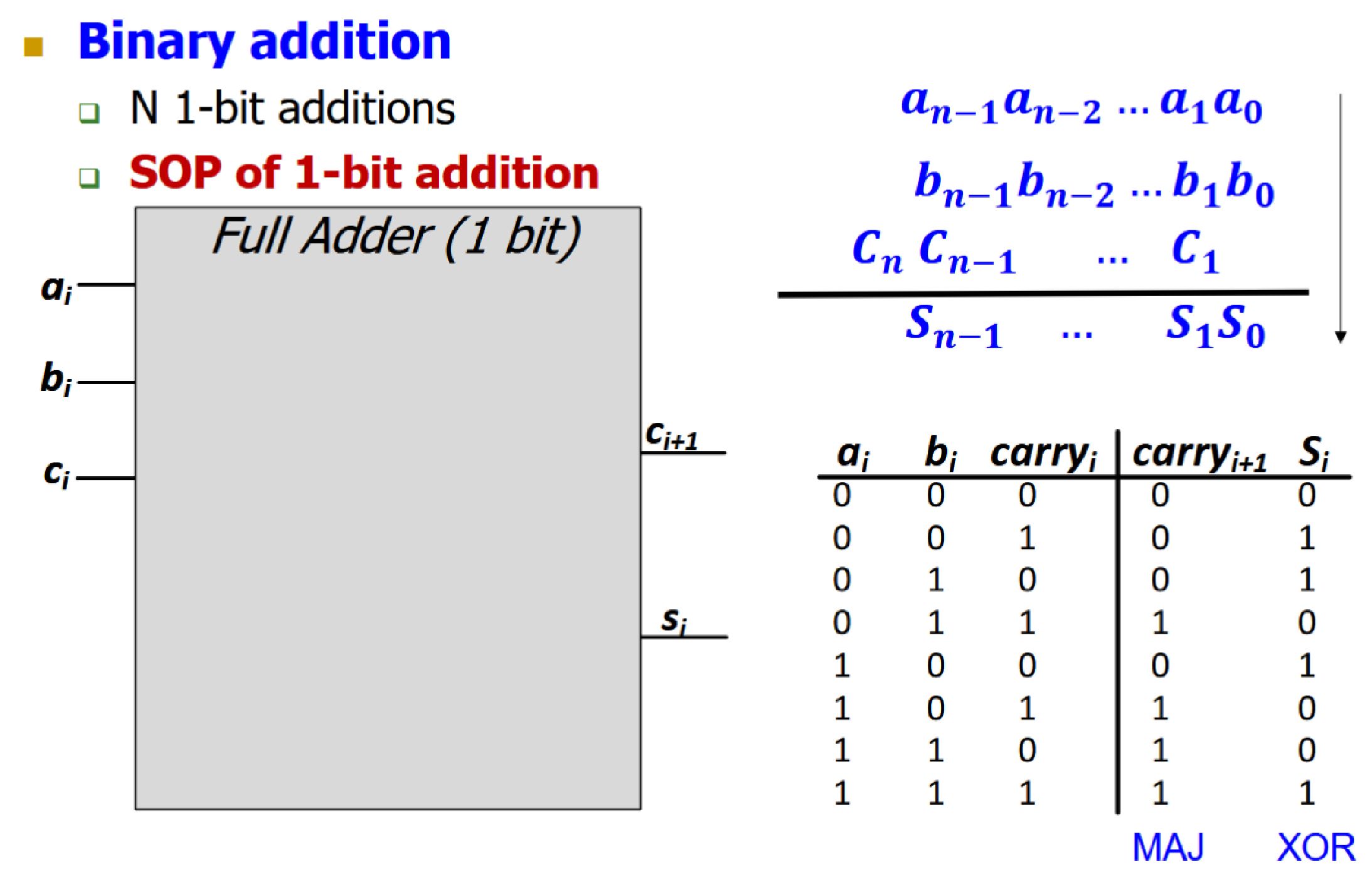
ETH::2._Semester::DDCA::03._Combinational_Logic_II_and_Sequential_Logic::1._Full_Adder
Full Adder
image-occlusion:rect:left=.8168:top=.9307:width=.1774:height=.0558:oi=1
Back
ETH::2._Semester::DDCA::03._Combinational_Logic_II_and_Sequential_Logic::1._Full_Adder
Full Adder
image-occlusion:rect:left=.8168:top=.9307:width=.1774:height=.0558:oi=1
Toggle Masks
Field-by-field Comparison
Field
Before
After
Occlusion {{c1::image-occlusion:rect:left=.8168:top=.9307:width=.1774:height=.0558:oi=1}}<br>
Image <img src="paste-8436c8f8af1bf260ebd78993c1d11a17c97c0dd2.jpg">
Header Full Adder
Tags:
ETH::2._Semester::DDCA::03._Combinational_Logic_II_and_Sequential_Logic::1._Full_Adder
Note 13: ETH::2. Semester::DDCA
Deck: ETH::2. Semester::DDCANote Type: Horvath ClassicGUID: e.w!.^HZQk
added
Previous
Note did not exist
New Note
Front
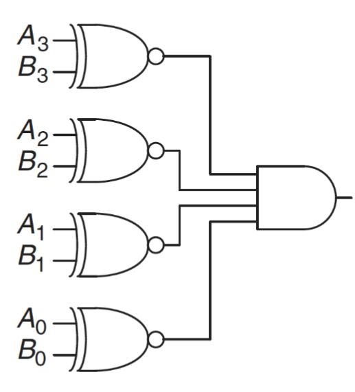
ETH::2._Semester::DDCA::03._Combinational_Logic_II_and_Sequential_Logic::4._Comparator
What is this?
Back
ETH::2._Semester::DDCA::03._Combinational_Logic_II_and_Sequential_Logic::4._Comparator
What is this?
An equality checker.
Field-by-field Comparison
Field
Before
After
Front What is this?<br><br><img src="paste-9ee9299a0aa47519e61e8ffe9cefcd2d2ffa51c2.jpg">
Back An equality checker.
Tags:
ETH::2._Semester::DDCA::03._Combinational_Logic_II_and_Sequential_Logic::4._Comparator
Note 14: ETH::2. Semester::DDCA
Deck: ETH::2. Semester::DDCANote Type: Horvath ClassicGUID: g-~*^Ki!(:
added
Previous
Note did not exist
New Note
Front
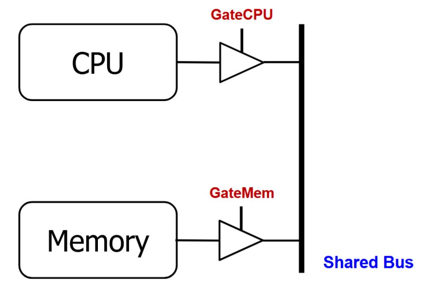
ETH::2._Semester::DDCA::03._Combinational_Logic_II_and_Sequential_Logic::6._Tri-State_Buffer
Imagine a wire connecting the CPU and memory. At any time only the CPU or the memory can place a value on the wire, both not both.
Back
ETH::2._Semester::DDCA::03._Combinational_Logic_II_and_Sequential_Logic::6._Tri-State_Buffer
Imagine a wire connecting the CPU and memory. At any time only the CPU or the memory can place a value on the wire, both not both.
You can have two tri-state buffers: one driven by CPU, the other memory; and ensure at most one is enabled at any time.
Field-by-field Comparison
Field
Before
After
Front Imagine a wire connecting the CPU and memory. At any time only the CPU or the memory can place a value on the wire, both not both.<br><br>How do we model this as a circuit?
Back You can have two tri-state buffers: one driven by CPU, the other memory; and ensure at most one is enabled at any time.<br><br><img src="paste-3e60268fdf3d3d4e9613807017fd11ee2dd4909f.jpg">
Tags:
ETH::2._Semester::DDCA::03._Combinational_Logic_II_and_Sequential_Logic::6._Tri-State_Buffer
Note 15: ETH::2. Semester::DDCA
Deck: ETH::2. Semester::DDCANote Type: Horvath ClassicGUID: g.dcXCwTR^
added
Previous
Note did not exist
New Note
Front
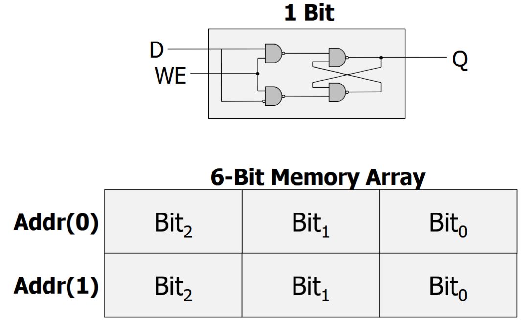
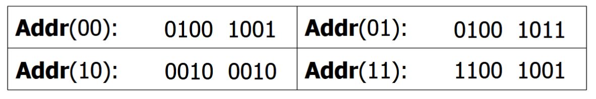
ETH::2._Semester::DDCA::03._Combinational_Logic_II_and_Sequential_Logic::15._Memory
How many locations and bits does this memory array have?
Back
ETH::2._Semester::DDCA::03._Combinational_Logic_II_and_Sequential_Logic::15._Memory
How many locations and bits does this memory array have?
4 locations X 3 bits
Field-by-field Comparison
Field
Before
After
Front How many locations and bits does this memory array have?<br><br><img src="paste-527c14fba71cb77a30a80a0db3ff30a5ca8a1b03.jpg">
Back 4 locations X 3 bits
Tags:
ETH::2._Semester::DDCA::03._Combinational_Logic_II_and_Sequential_Logic::15._Memory
Note 16: ETH::2. Semester::DDCA
Deck: ETH::2. Semester::DDCANote Type: Horvath ClassicGUID: g8HHZjvwjk
added
Previous
Note did not exist
New Note
Front
ETH::2._Semester::DDCA::03._Combinational_Logic_II_and_Sequential_Logic::13._The_Gated_D_Latch
How do we guarantee correct operation of an R-S Latch?
Back
ETH::2._Semester::DDCA::03._Combinational_Logic_II_and_Sequential_Logic::13._The_Gated_D_Latch
How do we guarantee correct operation of an R-S Latch?
We add two more NAND gates.
\(Q\) takes the value of \(D\), when write enable (WE) is set to 1.
\(S\) and \(R\) can never be 0 at the same time!
Field-by-field Comparison
Field
Before
After
Front How do we guarantee correct operation of an R-S Latch?
Back We add two more NAND gates.<br><br><img src="paste-75ed2b046c6dd5698e1016b588d9baa5ff3affdf.jpg"><br><br>\(Q\) takes the value of \(D\), when write enable (WE) is set to 1.<br>\(S\) and \(R\) can never be 0 at the same time!<br><br><img src="paste-d6a38ff36eeae6a05033cd1da3fa1f32da25717f.jpg">
Tags:
ETH::2._Semester::DDCA::03._Combinational_Logic_II_and_Sequential_Logic::13._The_Gated_D_Latch
Note 17: ETH::2. Semester::DDCA
Deck: ETH::2. Semester::DDCANote Type: Horvath ClassicGUID: h!H8&>iQx{
added
Previous
Note did not exist
New Note
Front
ETH::2._Semester::DDCA::03._Combinational_Logic_II_and_Sequential_Logic::2._The_Programmable_Logic_Array_(PLA)
How do we determine the number of OR gates in a PLA?
Back
ETH::2._Semester::DDCA::03._Combinational_Logic_II_and_Sequential_Logic::2._The_Programmable_Logic_Array_(PLA)
How do we determine the number of OR gates in a PLA?
The number of output columns in the truth table.
Field-by-field Comparison
Field
Before
After
Front How do we determine the number of OR gates in a PLA?
Back The number of output columns in the truth table.
Tags:
ETH::2._Semester::DDCA::03._Combinational_Logic_II_and_Sequential_Logic::2._The_Programmable_Logic_Array_(PLA)
Note 18: ETH::2. Semester::DDCA
Deck: ETH::2. Semester::DDCANote Type: Horvath ClassicGUID: iyge$&[U#_
added
Previous
Note did not exist
New Note
Front
ETH::2._Semester::DDCA::03._Combinational_Logic_II_and_Sequential_Logic::7._Logic_Simplification_using_Boolean_Algebra_Rules
What is this?
Back
ETH::2._Semester::DDCA::03._Combinational_Logic_II_and_Sequential_Logic::7._Logic_Simplification_using_Boolean_Algebra_Rules
What is this?
A priority circuit.
Inputs: "Requestors" with priority levels Outputs: "Grant" signal for each requestor
Field-by-field Comparison
Field
Before
After
Front What is this?<br><br><img src="paste-50fbc0b6a9081d2f896cc292f56cc4a470bd44ab.jpg">
Back A priority circuit.<br><ul><li>Inputs: "Requestors" with priority levels</li><li>Outputs: "Grant" signal for each requestor</li></ul>
Tags:
ETH::2._Semester::DDCA::03._Combinational_Logic_II_and_Sequential_Logic::7._Logic_Simplification_using_Boolean_Algebra_Rules
Note 19: ETH::2. Semester::DDCA
Deck: ETH::2. Semester::DDCANote Type: Horvath ClozeGUID: jY?vAb-}P$
added
Previous
Note did not exist
New Note
Front
ETH::2._Semester::DDCA::03._Combinational_Logic_II_and_Sequential_Logic::11._Basic_Element:_Cross-Coupled_Inverters
Pros and cons of other storage technology (flash memory, hard disk, tape)
Very cheap Much slower, access takes a long time, non-volatile
Back
ETH::2._Semester::DDCA::03._Combinational_Logic_II_and_Sequential_Logic::11._Basic_Element:_Cross-Coupled_Inverters
Pros and cons of other storage technology (flash memory, hard disk, tape)
Very cheap Much slower, access takes a long time, non-volatile
Field-by-field Comparison
Field
Before
After
Text Pros and cons of other storage technology (flash memory, hard disk, tape)<br><ul><li>{{c1::Very cheap}}</li><li>{{c2::Much slower, access takes a long time, non-volatile}}</li></ul>
Tags:
ETH::2._Semester::DDCA::03._Combinational_Logic_II_and_Sequential_Logic::11._Basic_Element:_Cross-Coupled_Inverters
Note 20: ETH::2. Semester::DDCA
Deck: ETH::2. Semester::DDCANote Type: Horvath ClassicGUID: kOBb
added
Previous
Note did not exist
New Note
Front
ETH::2._Semester::DDCA::03._Combinational_Logic_II_and_Sequential_Logic::6._Tri-State_Buffer
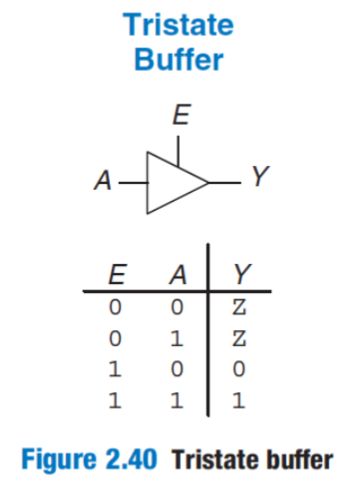
What does the Z mean here?
Back
ETH::2._Semester::DDCA::03._Combinational_Logic_II_and_Sequential_Logic::6._Tri-State_Buffer
What does the Z mean here?
Signal that is not driven by any circuit (e.g. open circuit, floating wire).
Field-by-field Comparison
Field
Before
After
Front What does the Z mean here?<br><br><img src="paste-6aad4a37bc003259212e2f00d56e604b0cf5c2b8.jpg">
Back Signal that is not driven by any circuit (e.g. open circuit, floating wire).
Tags:
ETH::2._Semester::DDCA::03._Combinational_Logic_II_and_Sequential_Logic::6._Tri-State_Buffer
Note 21: ETH::2. Semester::DDCA
Deck: ETH::2. Semester::DDCANote Type: Horvath ClassicGUID: kp|/N}vt~s
added
Previous
Note did not exist
New Note
Front
ETH::2._Semester::DDCA::03._Combinational_Logic_II_and_Sequential_Logic::2._The_Programmable_Logic_Array_(PLA)
How do we determine the number of AND gates in a PLA?
Back
ETH::2._Semester::DDCA::03._Combinational_Logic_II_and_Sequential_Logic::2._The_Programmable_Logic_Array_(PLA)
How do we determine the number of AND gates in a PLA?
For an n-input logic function, we need a PLA with 2ⁿ n-input AND gates.
Field-by-field Comparison
Field
Before
After
Front <div><strong>How do we determine the number of AND gates in a PLA?</strong></div>
Back For an n-input logic function, we need a PLA with 2ⁿ n-input AND gates.<br><strong><br>Remember SOP:</strong> the number of possible minterms
Tags:
ETH::2._Semester::DDCA::03._Combinational_Logic_II_and_Sequential_Logic::2._The_Programmable_Logic_Array_(PLA)
Note 22: ETH::2. Semester::DDCA
Deck: ETH::2. Semester::DDCANote Type: Horvath ClassicGUID: m6MCp)pX:Q
added
Previous
Note did not exist
New Note
Front
ETH::2._Semester::DDCA::03._Combinational_Logic_II_and_Sequential_Logic::7._Logic_Simplification_using_Boolean_Algebra_Rules
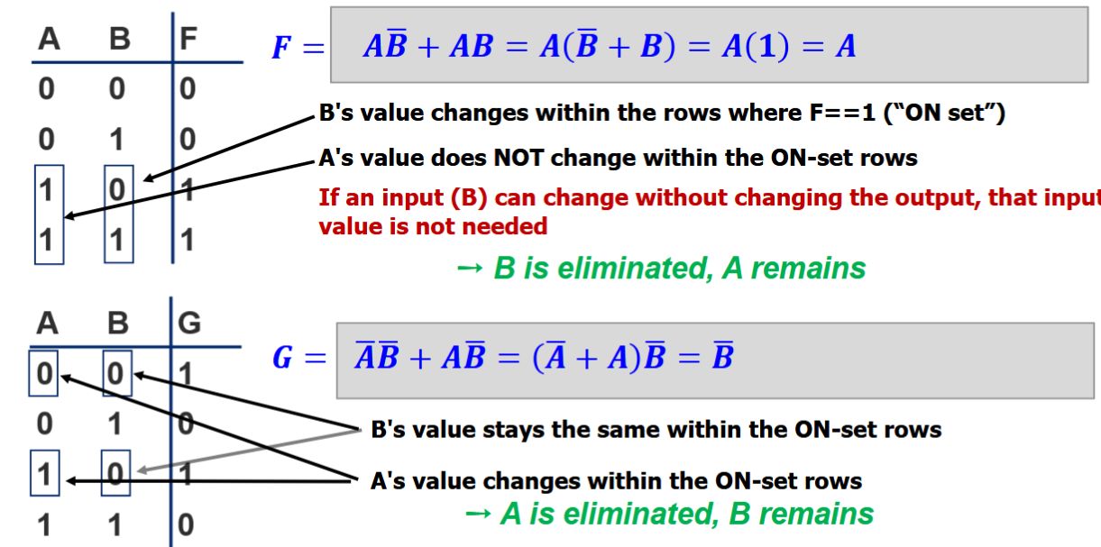
What is the Uniting Theorem?
Back
ETH::2._Semester::DDCA::03._Combinational_Logic_II_and_Sequential_Logic::7._Logic_Simplification_using_Boolean_Algebra_Rules
What is the Uniting Theorem?
\(F=A\overline B+AB\)
Field-by-field Comparison
Field
Before
After
Front What is the Uniting Theorem?
Back \(F=A\overline B+AB\)<br><br><img src="paste-544b792a3b0a0008ec05e73f83984d8d6b36adab.jpg">
Tags:
ETH::2._Semester::DDCA::03._Combinational_Logic_II_and_Sequential_Logic::7._Logic_Simplification_using_Boolean_Algebra_Rules
Note 23: ETH::2. Semester::DDCA
Deck: ETH::2. Semester::DDCANote Type: Horvath ClassicGUID: nZ:%JyRTd=
added
Previous
Note did not exist
New Note
Front
ETH::2._Semester::DDCA::03._Combinational_Logic_II_and_Sequential_Logic::15._Memory
Back
ETH::2._Semester::DDCA::03._Combinational_Logic_II_and_Sequential_Logic::15._Memory
What is Addressability?
The number of bits of information stored in each location.
E.g. here addressability is 8 bits.
Field-by-field Comparison
Field
Before
After
Front What is Addressability?
Back The number of bits of information stored in each location. <br><br>E.g. here addressability is 8 bits.<br><br><img src="paste-cdfafca1398985f93cea204a6b7b7073d008729e.jpg">
Tags:
ETH::2._Semester::DDCA::03._Combinational_Logic_II_and_Sequential_Logic::15._Memory
Note 24: ETH::2. Semester::DDCA
Deck: ETH::2. Semester::DDCANote Type: Horvath ClassicGUID: o3LWZaHF!=
added
Previous
Note did not exist
New Note
Front
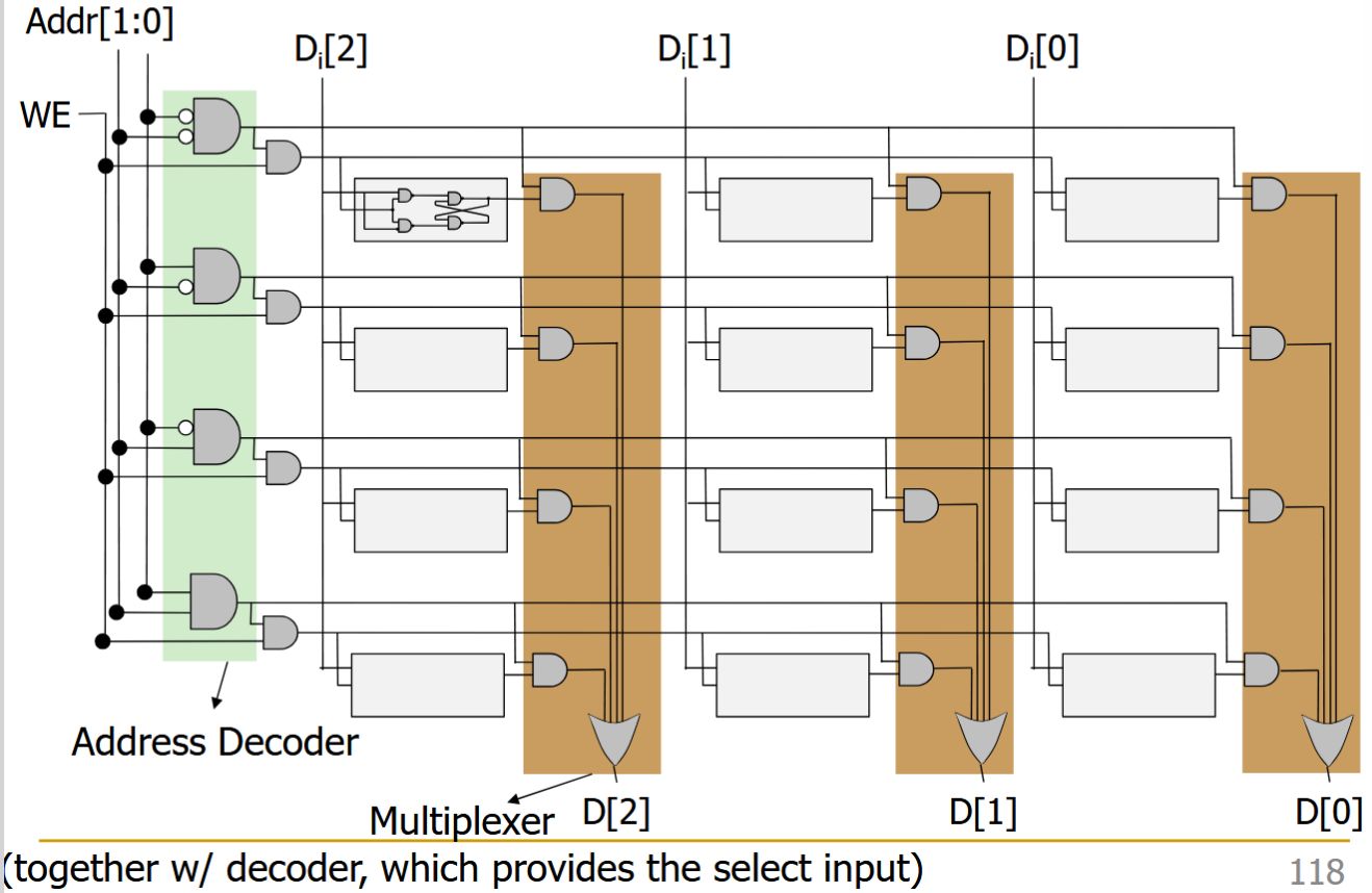
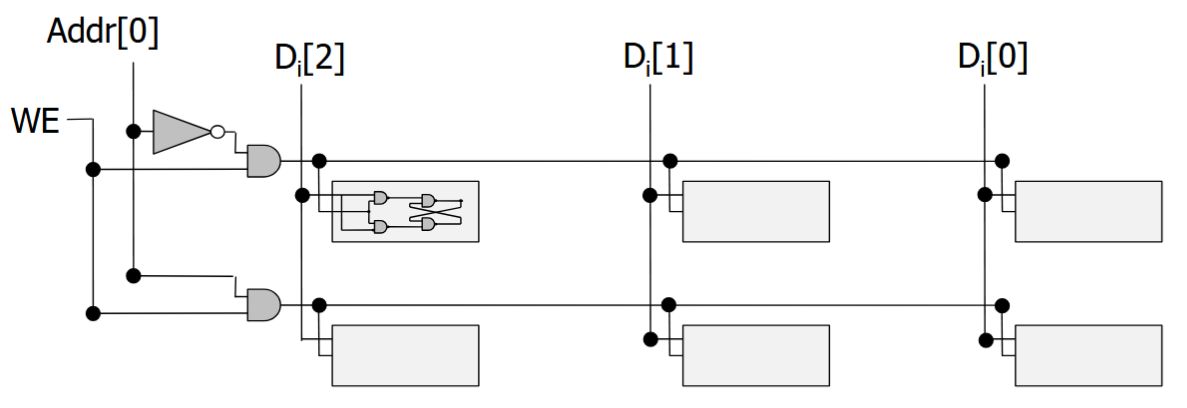
ETH::2._Semester::DDCA::03._Combinational_Logic_II_and_Sequential_Logic::15._Memory
Writing to Memory
What is \(D_i\) here?
Back
ETH::2._Semester::DDCA::03._Combinational_Logic_II_and_Sequential_Logic::15._Memory
Writing to Memory
What is \(D_i\) here?
Input.
Field-by-field Comparison
Field
Before
After
Front Writing to Memory<br><br>What is \(D_i\) here?<br><br><img src="paste-7e3105fcf0e2a3f5313495e28ac3d165f96c13ac.jpg">
Back Input.
Tags:
ETH::2._Semester::DDCA::03._Combinational_Logic_II_and_Sequential_Logic::15._Memory
Note 25: ETH::2. Semester::DDCA
Deck: ETH::2. Semester::DDCANote Type: Horvath ClassicGUID: padK$?kSq8
added
Previous
Note did not exist
New Note
Front
ETH::2._Semester::DDCA::03._Combinational_Logic_II_and_Sequential_Logic::2._The_Programmable_Logic_Array_(PLA)
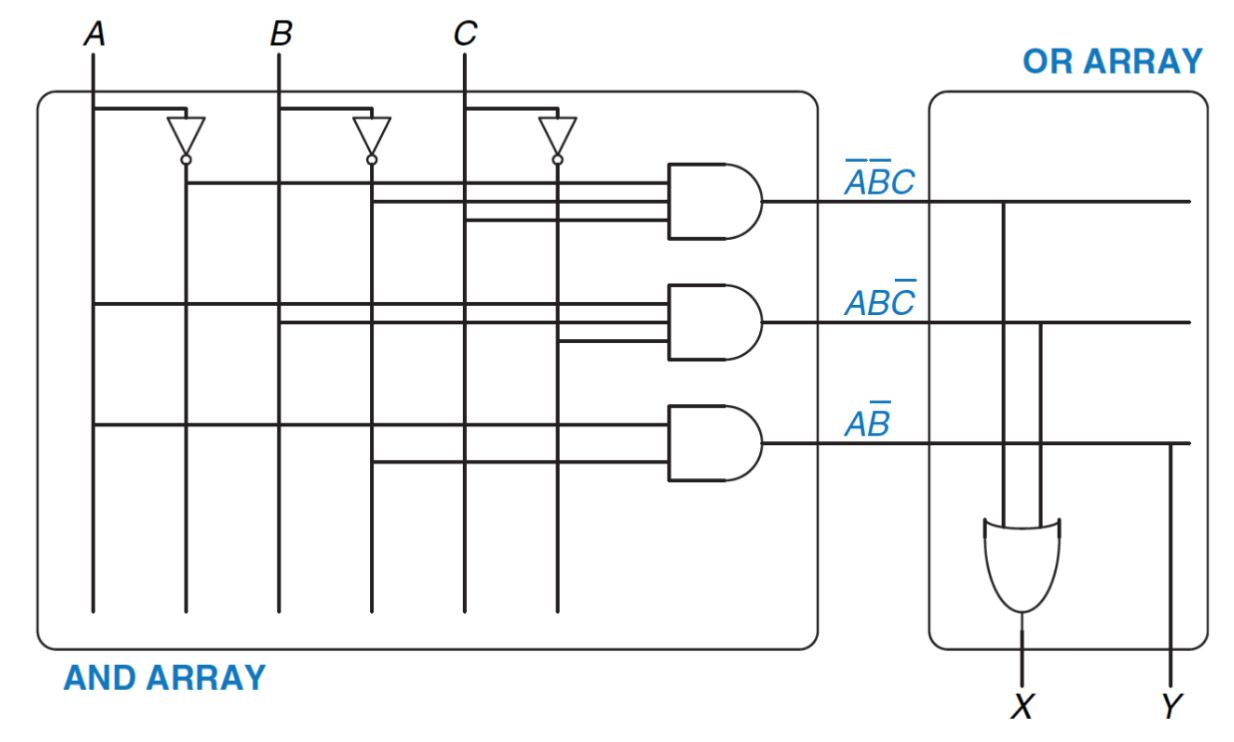
How do we implement a logic function in a PLA?
Back
ETH::2._Semester::DDCA::03._Combinational_Logic_II_and_Sequential_Logic::2._The_Programmable_Logic_Array_(PLA)
How do we implement a logic function in a PLA?
Connect the output of an AND gate to the input of an OR gate if the corresponding minterm is included in the SOP.
This is a simple programmable logic construct.
Field-by-field Comparison
Field
Before
After
Front How do we implement a logic function in a PLA?
Back Connect the output of an AND gate to the input of an OR gate if the corresponding minterm is included in the SOP.<br><br>This is a simple programmable logic construct.<br><br><img src="paste-2fbd7177ca3914ec569c4d1587320498ff0c8fa1.jpg">
Tags:
ETH::2._Semester::DDCA::03._Combinational_Logic_II_and_Sequential_Logic::2._The_Programmable_Logic_Array_(PLA)
Note 26: ETH::2. Semester::DDCA
Deck: ETH::2. Semester::DDCANote Type: Horvath ClozeGUID: q)njawwNYM
added
Previous
Note did not exist
New Note
Front
ETH::2._Semester::DDCA::03._Combinational_Logic_II_and_Sequential_Logic::6._Tri-State_Buffer
A tri-state buffer enables gating of different signals onto a wire .
Back
ETH::2._Semester::DDCA::03._Combinational_Logic_II_and_Sequential_Logic::6._Tri-State_Buffer
A tri-state buffer enables gating of different signals onto a wire .
It acts like a switch.
Field-by-field Comparison
Field
Before
After
Text A tri-state buffer enables {{c1::gating of different signals onto a wire}}.
Extra <img src="paste-6aad4a37bc003259212e2f00d56e604b0cf5c2b8.jpg"><br><br>It acts like a switch.
Tags:
ETH::2._Semester::DDCA::03._Combinational_Logic_II_and_Sequential_Logic::6._Tri-State_Buffer
Note 27: ETH::2. Semester::DDCA
Deck: ETH::2. Semester::DDCANote Type: Horvath ClozeGUID: q,=4BpC=Eo
added
Previous
Note did not exist
New Note
Front
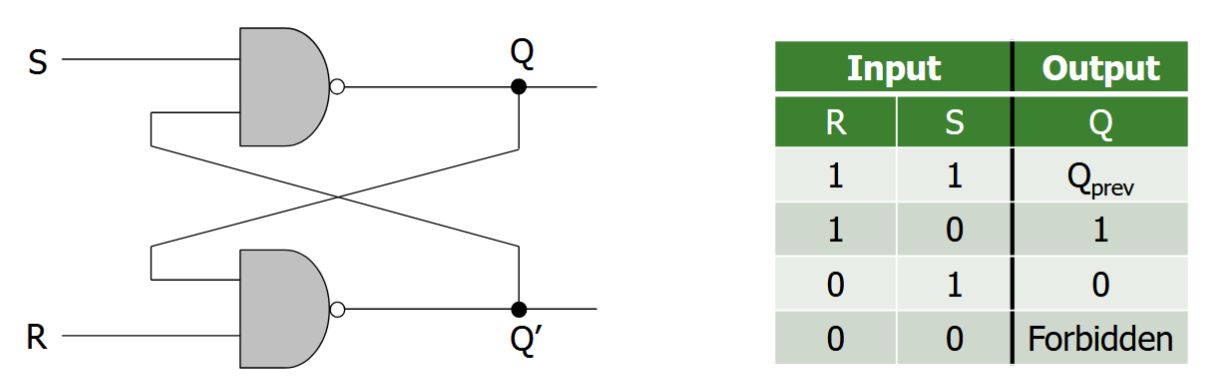
ETH::2._Semester::DDCA::03._Combinational_Logic_II_and_Sequential_Logic::12._Basic_Storage_Element:_The_R-S_Latch
R-S Latch
Data is stored at Q (inverse at Q') S and R are control inputs
In quiescent(idle) state, both S and R are held at 1 S (set): drive S to 0 (keeping R at 1) to change Q to 1 R (reset): drive R to 0 (keeping S at 1) to change Q to 0
Back
ETH::2._Semester::DDCA::03._Combinational_Logic_II_and_Sequential_Logic::12._Basic_Storage_Element:_The_R-S_Latch
R-S Latch
Data is stored at Q (inverse at Q') S and R are control inputs
In quiescent(idle) state, both S and R are held at 1 S (set): drive S to 0 (keeping R at 1) to change Q to 1 R (reset): drive R to 0 (keeping S at 1) to change Q to 0 S and R should not both be 0 at the same time.
Field-by-field Comparison
Field
Before
After
Text R-S Latch<br><ul><li>Data is stored at {{c1::Q (inverse at Q')}}</li><li>S and R are {{c2::control inputs}}</li><ul>
<li>In quiescent(idle) state, {{c3::both S and R are held at 1}}</li><li>S (set): {{c4::drive S to 0 (keeping R at 1) to change Q to 1}}</li><li>R (reset): {{c4::drive R to 0 (keeping S at 1) to change Q to 0}}</li></ul></ul>
Extra <img src="paste-d484990009a33988ad2d3a060d667ec92928c41c.jpg"><br><br>S and R should not both be 0 at the same time.
Tags:
ETH::2._Semester::DDCA::03._Combinational_Logic_II_and_Sequential_Logic::12._Basic_Storage_Element:_The_R-S_Latch
Note 28: ETH::2. Semester::DDCA
Deck: ETH::2. Semester::DDCANote Type: Horvath ClozeGUID: qks
added
Previous
Note did not exist
New Note
Front
ETH::2._Semester::DDCA::03._Combinational_Logic_II_and_Sequential_Logic::3._Logical_Completeness
The set of gates {AND, OR, NOT} is logically complete because we can build a circuit to carry out the specification of any truth table we wish, without using any other kind of gate.
Back
ETH::2._Semester::DDCA::03._Combinational_Logic_II_and_Sequential_Logic::3._Logical_Completeness
The set of gates {AND, OR, NOT} is logically complete because we can build a circuit to carry out the specification of any truth table we wish, without using any other kind of gate.
Field-by-field Comparison
Field
Before
After
Text The set of gates {AND, OR, NOT} is {{c1::logically complete}} because we can build a circuit to carry out the specification of any truth table we wish, without using any other kind of gate.
Tags:
ETH::2._Semester::DDCA::03._Combinational_Logic_II_and_Sequential_Logic::3._Logical_Completeness
Note 29: ETH::2. Semester::DDCA
Deck: ETH::2. Semester::DDCANote Type: Horvath ClozeGUID: s>dpZ2?aZt
added
Previous
Note did not exist
New Note
Front
ETH::2._Semester::DDCA::03._Combinational_Logic_II_and_Sequential_Logic::15._Memory
Memory is comprised of locations that can be written to or read from.
Back
ETH::2._Semester::DDCA::03._Combinational_Logic_II_and_Sequential_Logic::15._Memory
Memory is comprised of locations that can be written to or read from.
Field-by-field Comparison
Field
Before
After
Text {{c1::Memory}} is comprised of locations that can be written to or read from.
Tags:
ETH::2._Semester::DDCA::03._Combinational_Logic_II_and_Sequential_Logic::15._Memory
Note 30: ETH::2. Semester::DDCA
Deck: ETH::2. Semester::DDCANote Type: Horvath ClozeGUID: sc1PEC3C0X
added
Previous
Note did not exist
New Note
Front
ETH::2._Semester::DDCA::03._Combinational_Logic_II_and_Sequential_Logic::15._Memory
The entire set of unique locations in memory is referred to as the address space .
Back
ETH::2._Semester::DDCA::03._Combinational_Logic_II_and_Sequential_Logic::15._Memory
The entire set of unique locations in memory is referred to as the address space .
Field-by-field Comparison
Field
Before
After
Text The entire set of unique locations in memory is referred to as {{c1::the address space}}.
Tags:
ETH::2._Semester::DDCA::03._Combinational_Logic_II_and_Sequential_Logic::15._Memory
Note 31: ETH::2. Semester::DDCA
Deck: ETH::2. Semester::DDCANote Type: Horvath ClassicGUID: spIlS+D;j=
added
Previous
Note did not exist
New Note
Front
ETH::2._Semester::DDCA::03._Combinational_Logic_II_and_Sequential_Logic::12._Basic_Storage_Element:_The_R-S_Latch
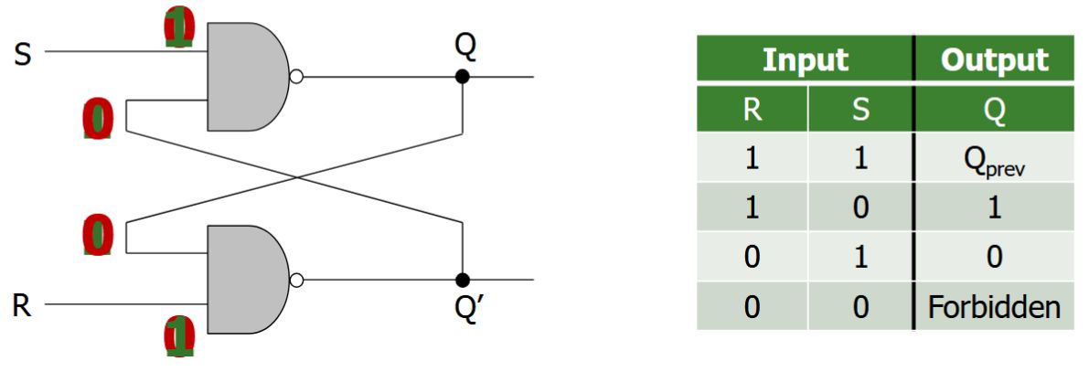
Why is \(R=S=0\) illegal in a R-S Latch?
Back
ETH::2._Semester::DDCA::03._Combinational_Logic_II_and_Sequential_Logic::12._Basic_Storage_Element:_The_R-S_Latch
Why is \(R=S=0\) illegal in a R-S Latch?
If \(R=S=0\), \(Q\) and \(Q'\) will both settle to 1, which breaks our invariant that \(Q \neq Q'\).
If \(S\) and \(R\) transition back to 1 at the same time, \(Q\) and \(Q'\) begin to oscillate between 1 and 0 because their final values depend on each other (metastability ).
This eventually settles depending on variation in the circuits (more on this in the Timing Lecture ).
Field-by-field Comparison
Field
Before
After
Front Why is \(R=S=0\) illegal in a R-S Latch?<br><br><img src="paste-e939b3a4513b1cd81fee9957735bc8b234d94d58.jpg">
Back <div>If \(R=S=0\), \(Q\) and \(Q'\) will both settle to 1, which <b>breaks</b> our invariant that \(Q \neq Q'\).</div><div><strong><br></strong></div>
<div>If \(S\) and \(R\) transition back to 1 at the same time, \(Q\) and \(Q'\) begin to oscillate between 1 and 0 because their final values depend on each other (<strong>metastability</strong>).</div><div><br></div><div>This eventually settles depending on <strong>variation in the circuits</strong> (more on this in the <strong>Timing Lecture</strong>).</div>
Tags:
ETH::2._Semester::DDCA::03._Combinational_Logic_II_and_Sequential_Logic::12._Basic_Storage_Element:_The_R-S_Latch
Note 32: ETH::2. Semester::DDCA
Deck: ETH::2. Semester::DDCANote Type: Horvath ClassicGUID: w,kFo*OkK6
added
Previous
Note did not exist
New Note
Front
ETH::2._Semester::DDCA::03._Combinational_Logic_II_and_Sequential_Logic::11._Basic_Element:_Cross-Coupled_Inverters
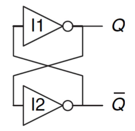
What is this?
Back
ETH::2._Semester::DDCA::03._Combinational_Logic_II_and_Sequential_Logic::11._Basic_Element:_Cross-Coupled_Inverters
What is this?
Cross-Coupled Inverters.
Has two stable states: \(Q=1\) or \(Q=0\).
Has a third possible "metastable" state with both outputs oscillating between 0 and 1 (we will see this later).
Not useful without a
control mechanism for setting Q.
Field-by-field Comparison
Field
Before
After
Front What is this?<br><br><img src="paste-efd9c52b653ff9b4a9524a61121fca9066d0842e.jpg">
Back Cross-Coupled Inverters.<br><br>Has two stable states: \(Q=1\) or \(Q=0\).<br>Has a third possible "metastable" state with both outputs oscillating between 0 and 1 (we will see this later).<br><br>Not useful without a <b>control mechanism </b>for setting Q.<br><br><img src="paste-40fef199fe312874c26dd3080f9b553c5504e4ee.jpg">
Tags:
ETH::2._Semester::DDCA::03._Combinational_Logic_II_and_Sequential_Logic::11._Basic_Element:_Cross-Coupled_Inverters
Note 33: ETH::2. Semester::DDCA
Deck: ETH::2. Semester::DDCANote Type: Horvath ClassicGUID: w0Wk-s@q$K
added
Previous
Note did not exist
New Note
Front
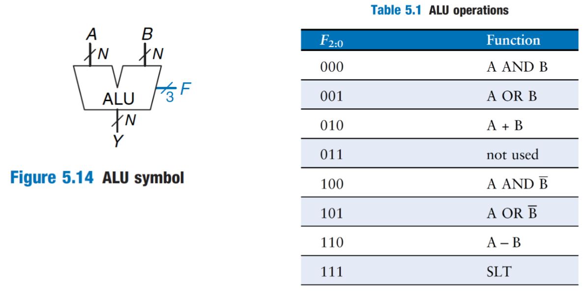
ETH::2._Semester::DDCA::03._Combinational_Logic_II_and_Sequential_Logic::5._ALU_(Arithmetic_Logic_Unit)
Back
ETH::2._Semester::DDCA::03._Combinational_Logic_II_and_Sequential_Logic::5._ALU_(Arithmetic_Logic_Unit)
What does an ALU do?
It combines a variety of arithmetic and logical operations into a single unit (that performs only one function at a time).
Field-by-field Comparison
Field
Before
After
Front What does an ALU do?
Back It combines a variety of arithmetic and logical operations into a single unit (that performs only one function at a time).<br><br><img src="paste-d4c76084858a27a2bc15385a19ee00e24b7fc095.jpg">
Tags:
ETH::2._Semester::DDCA::03._Combinational_Logic_II_and_Sequential_Logic::5._ALU_(Arithmetic_Logic_Unit)
Note 34: ETH::2. Semester::DDCA
Deck: ETH::2. Semester::DDCANote Type: Horvath ClozeGUID: wK&dW+a*q9
added
Previous
Note did not exist
New Note
Front
ETH::2._Semester::DDCA::03._Combinational_Logic_II_and_Sequential_Logic::3._Logical_Completeness
NAND and NOR are logically complete .
Back
ETH::2._Semester::DDCA::03._Combinational_Logic_II_and_Sequential_Logic::3._Logical_Completeness
NAND and NOR are logically complete .
Field-by-field Comparison
Field
Before
After
Text NAND and NOR are {{c1::logically complete}}.
Tags:
ETH::2._Semester::DDCA::03._Combinational_Logic_II_and_Sequential_Logic::3._Logical_Completeness
Note 35: ETH::2. Semester::DDCA
Deck: ETH::2. Semester::DDCANote Type: Horvath OcclusioGUID: y6L!`3rg+h
added
Previous
Note did not exist
New Note
Front
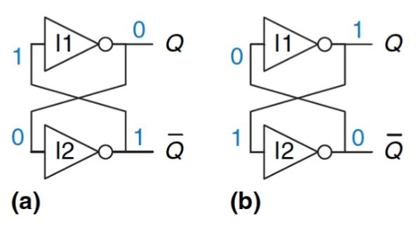
ETH::2._Semester::DDCA::03._Combinational_Logic_II_and_Sequential_Logic::17._Sequential_Logic_Circuits
What's the difference between these two?
image-occlusion:rect:left=.0066:top=.7908:width=.9822:height=.1903
Back
ETH::2._Semester::DDCA::03._Combinational_Logic_II_and_Sequential_Logic::17._Sequential_Logic_Circuits
What's the difference between these two?
image-occlusion:rect:left=.0066:top=.7908:width=.9822:height=.1903
Toggle Masks
Field-by-field Comparison
Field
Before
After
Occlusion {{c1::image-occlusion:rect:left=.0066:top=.7908:width=.9822:height=.1903}}<br>
Image <img src="paste-56ccd7a0fecaeb262dc5922a407d2ee8a4c16d37.jpg">
Header What's the difference between these two?
Tags:
ETH::2._Semester::DDCA::03._Combinational_Logic_II_and_Sequential_Logic::17._Sequential_Logic_Circuits
Note 36: ETH::2. Semester::DDCA
Deck: ETH::2. Semester::DDCANote Type: Horvath ClozeGUID: yixUKU?m~)
added
Previous
Note did not exist
New Note
Front
ETH::2._Semester::DDCA::03._Combinational_Logic_II_and_Sequential_Logic::7._Logic_Simplification_using_Boolean_Algebra_Rules
Essence of Simplificationeliminated !
Back
ETH::2._Semester::DDCA::03._Combinational_Logic_II_and_Sequential_Logic::7._Logic_Simplification_using_Boolean_Algebra_Rules
Essence of Simplificationeliminated !
Field-by-field Comparison
Field
Before
After
Text Essence of Simplification<br><br>Find two-element subsets of the ON-set where only one variable changes its value. This single varying variable can be {{c1::eliminated}}!
Tags:
ETH::2._Semester::DDCA::03._Combinational_Logic_II_and_Sequential_Logic::7._Logic_Simplification_using_Boolean_Algebra_Rules