\[\sum_{k = 1}^n \binom{n}{k} = 2^n \]
Note 1: ETH::2. Semester::A&W
Deck: ETH::2. Semester::A&W
Note Type: Horvath Cloze
GUID:
added
Note Type: Horvath Cloze
GUID:
FwGQ#H|>Ez
Previous
Note did not exist
New Note
Front
Back
\[\sum_{k = 1}^n \binom{n}{k} = 2^n \]
Field-by-field Comparison
| Field | Before | After |
|---|---|---|
| Text | \[\sum_{k = 1}^n \binom{n}{k} = {{c1:: 2^n }}\] |
Note 2: ETH::2. Semester::Analysis
Deck: ETH::2. Semester::Analysis
Note Type: Horvath Cloze
GUID:
added
Note Type: Horvath Cloze
GUID:
MtKk|s)sx.
Previous
Note did not exist
New Note
Front
\(1 + x \le e^x\) oft nützlich.
Back
\(1 + x \le e^x\) oft nützlich.
Field-by-field Comparison
| Field | Before | After |
|---|---|---|
| Text | \(1 + x \le {{c1::e^x::Exponential}}\) oft nützlich. |
Note 3: ETH::2. Semester::DDCA
Deck: ETH::2. Semester::DDCA
Note Type: Horvath Cloze
GUID:
added
Note Type: Horvath Cloze
GUID:
&EOudn7bc
Previous
Note did not exist
New Note
Front
An FSM pictorially shows:
- the set of all possible states that a system can be in
- how the system transitions from one state to another
Back
An FSM pictorially shows:
- the set of all possible states that a system can be in
- how the system transitions from one state to another
Field-by-field Comparison
| Field | Before | After |
|---|---|---|
| Text | An FSM pictorially shows:<br><ol><li>{{c1::the set of all possible states that a system can be in}}</li><li>{{c2::how the system transitions from one state to another}}<br></li></ol> |
Note 4: ETH::2. Semester::DDCA
Deck: ETH::2. Semester::DDCA
Note Type: Horvath Cloze
GUID:
added
Note Type: Horvath Cloze
GUID:
*#UndBD{e
Previous
Note did not exist
New Note
Front
A sequential lock is an asynchronous "machine"
Back
A sequential lock is an asynchronous "machine"
State transitions can take place immediately in response to input.
There is nothing that synchronizes when each state transition must occur.
There is nothing that synchronizes when each state transition must occur.
Field-by-field Comparison
| Field | Before | After |
|---|---|---|
| Text | A sequential lock is an {{c1::asynchronous}} "machine" | |
| Extra | State transitions can take place immediately in response to input.<br><br>There is nothing that synchronizes when each state transition must occur. |
Note 5: ETH::2. Semester::DDCA
Deck: ETH::2. Semester::DDCA
Note Type: Horvath Cloze
GUID:
added
Note Type: Horvath Cloze
GUID:
AG/0U&~#@P
Previous
Note did not exist
New Note
Front
\(N\) locations require \(\log_2 N\) address bits.
Back
\(N\) locations require \(\log_2 N\) address bits.
log[#locations]
Field-by-field Comparison
| Field | Before | After |
|---|---|---|
| Text | \(N\) locations require {{c1::\(\log_2 N\)}} address bits. | |
| Extra | log[#locations] |
Note 6: ETH::2. Semester::DDCA
Deck: ETH::2. Semester::DDCA
Note Type: Horvath Classic
GUID:
added
Note Type: Horvath Classic
GUID:
AJ~67I*]U=
Previous
Note did not exist
New Note
Front
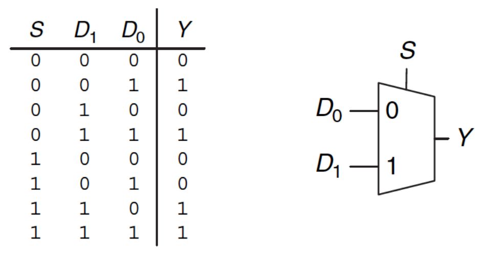
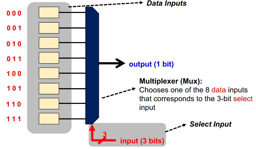
How does a multiplexer/selector work?
Back
How does a multiplexer/selector work?
Selects one of the \(N\) inputs to connect it to the output, based on the value of a \(\log_2 N\)-bit control input called select.
Example: 2-to-1 MUX
Field-by-field Comparison
| Field | Before | After |
|---|---|---|
| Front | How does a multiplexer/selector work? | |
| Back | <div>Selects one of the \(N\) inputs to connect it to the output, based on the value of a \(\log_2 N\)-bit control input called select.</div><div><br></div><div>Example: 2-to-1 MUX</div><div><br></div><div><img src="paste-8208411dc677e909d56e87886f8feebb89586c22.jpg"><br></div> |
Note 7: ETH::2. Semester::DDCA
Deck: ETH::2. Semester::DDCA
Note Type: Horvath Cloze
GUID:
added
Note Type: Horvath Cloze
GUID:
AOh7q@y=Z&
Previous
Note did not exist
New Note
Front
A flip-flop is called an edge-triggered state element because it captures data on the clock edge.
Back
A flip-flop is called an edge-triggered state element because it captures data on the clock edge.
A latch is a level-triggered state element.
Field-by-field Comparison
| Field | Before | After |
|---|---|---|
| Text | A flip-flop is called an {{c1::edge-triggered state element}} because it captures data on the clock edge. | |
| Extra | A latch is a level-triggered state element. |
Note 8: ETH::2. Semester::DDCA
Deck: ETH::2. Semester::DDCA
Note Type: Horvath Cloze
GUID:
added
Note Type: Horvath Cloze
GUID:
B8FT@NiVSO
Previous
Note did not exist
New Note
Front
Pros and cons of Dynamic RAM (DRAM)
- Cheap (one bit costs only one transistor plus one capacitor)
- Slower, reading destroys content (refresh), needs special process for manufacturing
Back
Pros and cons of Dynamic RAM (DRAM)
- Cheap (one bit costs only one transistor plus one capacitor)
- Slower, reading destroys content (refresh), needs special process for manufacturing
Field-by-field Comparison
| Field | Before | After |
|---|---|---|
| Text | Pros and cons of Dynamic RAM (DRAM)<ul><li>{{c1::Cheap (one bit costs only one transistor plus one capacitor)}}</li><li>{{c2::Slower, reading destroys content (refresh), needs special process for manufacturing}}</li></ul> |
Note 9: ETH::2. Semester::DDCA
Deck: ETH::2. Semester::DDCA
Note Type: Horvath Cloze
GUID:
added
Note Type: Horvath Cloze
GUID:
Bkh_O*c@~J
Previous
Note did not exist
New Note
Front
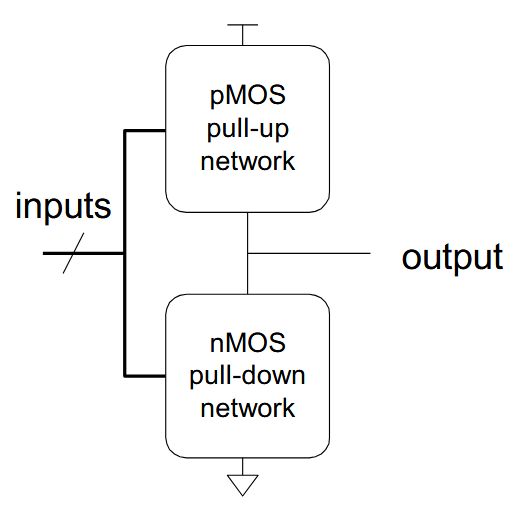
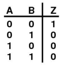
If both networks are OFF at the same time, the output is floating → undefined.
Back
If both networks are OFF at the same time, the output is floating → undefined.
Field-by-field Comparison
| Field | Before | After |
|---|---|---|
| Text | <img src="paste-a3eb18d4f8b16544780bf296d94ae3cb0386642d.jpg"><br><br> <div>If both networks are OFF at the same time, {{c1::the output is <strong>floating</strong> → undefined}}.</div> |
Note 10: ETH::2. Semester::DDCA
Deck: ETH::2. Semester::DDCA
Note Type: Horvath Cloze
GUID:
added
Note Type: Horvath Cloze
GUID:
BvCgV;{r@Y
Previous
Note did not exist
New Note
Front
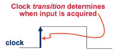
A clock is a general mechanism that triggers transition from one state to another in a (synchronous) sequential circuit.
Back
A clock is a general mechanism that triggers transition from one state to another in a (synchronous) sequential circuit.
Field-by-field Comparison
| Field | Before | After |
|---|---|---|
| Text | A {{c1::clock}} is a general mechanism that triggers transition from one state to another in a (synchronous) sequential circuit. |
Note 11: ETH::2. Semester::DDCA
Deck: ETH::2. Semester::DDCA
Note Type: Horvath Cloze
GUID:
added
Note Type: Horvath Cloze
GUID:
B}b_Cs$Q2`
Previous
Note did not exist
New Note
Front
The duality property states that we can swap OR and AND, 1 and 0 in an equation and it still is true.
Back
The duality property states that we can swap OR and AND, 1 and 0 in an equation and it still is true.
\(\overline{(AB)} = \overline{A} + \overline{B} \) gives \(\overline{(A + B)} = \overline{A} \overline{B}\)
Field-by-field Comparison
| Field | Before | After |
|---|---|---|
| Text | The duality property states that {{c1:: we can swap OR and AND, 1 and 0}} in an equation and it still is true. | |
| Extra | \(\overline{(AB)} = \overline{A} + \overline{B} \) gives \(\overline{(A + B)} = \overline{A} \overline{B}\) |
Note 12: ETH::2. Semester::DDCA
Deck: ETH::2. Semester::DDCA
Note Type: Horvath Classic
GUID:
added
Note Type: Horvath Classic
GUID:
C#j%f~ZG_/
Previous
Note did not exist
New Note
Front
What's static power consumption?
Back
What's static power consumption?
Power used when signals do not change.
Field-by-field Comparison
| Field | Before | After |
|---|---|---|
| Front | What's static power consumption? | |
| Back | Power used when signals do not change. |
Note 13: ETH::2. Semester::DDCA
Deck: ETH::2. Semester::DDCA
Note Type: Horvath Classic
GUID:
added
Note Type: Horvath Classic
GUID:
C=t{~$lGP^
Previous
Note did not exist
New Note
Front
What is this?
Back
What is this?
A NOT gate/inverter.
The bubble indicates inversion.
The bubble indicates inversion.
Field-by-field Comparison
| Field | Before | After |
|---|---|---|
| Front | What is this?<br><br><img src="paste-ac931ff5d7f389ff58099975d1f3a0ad8ab4c537.jpg"> | |
| Back | A NOT gate/inverter.<br><br><img src="paste-0ad43f42d4ff2676978fd7a8c28ab976a068e58b.jpg"><br><br>The bubble indicates inversion. |
Note 14: ETH::2. Semester::DDCA
Deck: ETH::2. Semester::DDCA
Note Type: Horvath Classic
GUID:
added
Note Type: Horvath Classic
GUID:
D[owgbdJ
Previous
Note did not exist
New Note
Front
What is this?
Back
What is this?
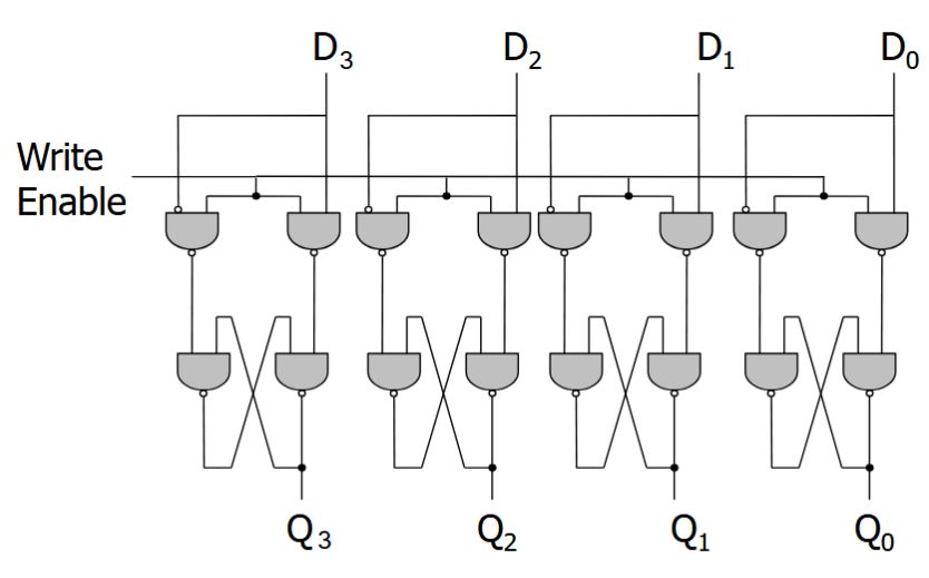
Here we have a register.
- It's a structure that stores more than one bit and can be read from and written to.
- Note that there is a single WE signal for all latches for simultaneous writes.
- This register holds 4 bits, and its data is referenced as Q[3:0].
Field-by-field Comparison
| Field | Before | After |
|---|---|---|
| Front | What is this?<br><br><img src="paste-be78c3f8e3954dfc7609bb2b8a3310972620f5c8.jpg"> | |
| Back | Here we have a <b>register.</b><br><ul><li>It's a structure that stores more than one bit and can be read from and written to.</li><li>Note that there is a single WE signal for all latches for simultaneous writes.</li><li>This register holds 4 bits, and its data is referenced as Q[3:0].</li></ul> |
Note 15: ETH::2. Semester::DDCA
Deck: ETH::2. Semester::DDCA
Note Type: Horvath Cloze
GUID:
added
Note Type: Horvath Cloze
GUID:
GIu2UZfi4!
Previous
Note did not exist
New Note
Front
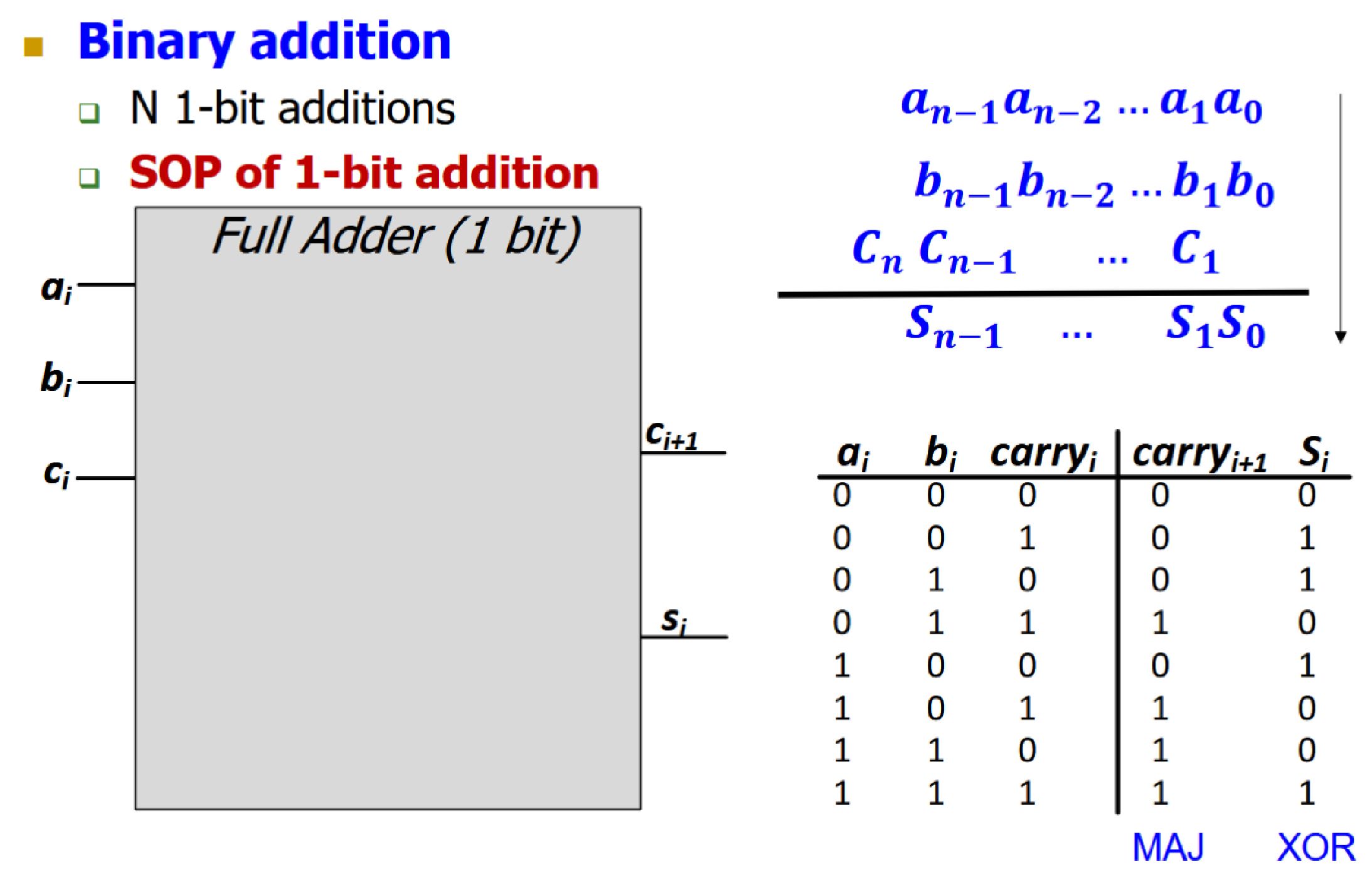
What does the "functional" in functional specification signify?
- Unique mapping from input values to output values
- The same input values produce the same output value every time.
- No memory (output does not depend on past input values)
Back
What does the "functional" in functional specification signify?
- Unique mapping from input values to output values
- The same input values produce the same output value every time.
- No memory (output does not depend on past input values)
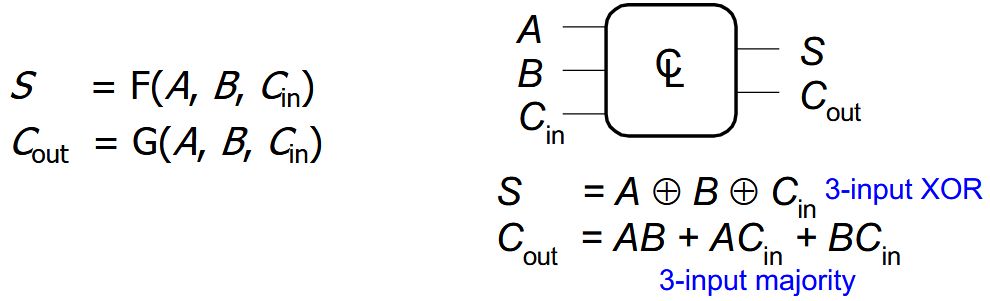
Example: Full 1-bit adder
Field-by-field Comparison
| Field | Before | After |
|---|---|---|
| Text | What does the "functional" in functional specification signify?<br><ol><li>{{c1::Unique mapping from input values to output values}}<br></li><li>{{c1::The same input values produce the same output value every time.}}<br></li><li>{{c1::No memory (output does not depend on past input values)}}<br></li></ol> | |
| Extra | Example: Full 1-bit adder<br><br><img src="paste-b9d2e36783cfe71ff832f7489428344e8584afc2.jpg"> |
Note 16: ETH::2. Semester::DDCA
Deck: ETH::2. Semester::DDCA
Note Type: Horvath Cloze
GUID:
added
Note Type: Horvath Cloze
GUID:
GJkgZHl?j0
Previous
Note did not exist
New Note
Front
Combinational Logic, as opposed to Sequential Logic, is memoryless.
Back
Combinational Logic, as opposed to Sequential Logic, is memoryless.
Outputs are strictly dependent on the combination of input values that are being applied to circuit right now.
Field-by-field Comparison
| Field | Before | After |
|---|---|---|
| Text | Combinational Logic, as opposed to Sequential Logic, is {{c1::memoryless}}. | |
| Extra | Outputs are strictly dependent on the combination of input values that are being applied to circuit <i>right now</i>. |
Note 17: ETH::2. Semester::DDCA
Deck: ETH::2. Semester::DDCA
Note Type: Horvath Cloze
GUID:
added
Note Type: Horvath Cloze
GUID:
GT1cT:#V..
Previous
Note did not exist
New Note
Front
Pros and cons of Static RAM (SRAM)
- Relatively fast
- Expensive (one bit costs 6+ transistors)
Back
Pros and cons of Static RAM (SRAM)
- Relatively fast
- Expensive (one bit costs 6+ transistors)
Field-by-field Comparison
| Field | Before | After |
|---|---|---|
| Text | Pros and cons of Static RAM (SRAM)<br><ul><li>{{c1::Relatively fast}}</li><li>{{c2::Expensive (one bit costs 6+ transistors)}}</li></ul> |
Note 18: ETH::2. Semester::DDCA
Deck: ETH::2. Semester::DDCA
Note Type: Horvath Cloze
GUID:
added
Note Type: Horvath Cloze
GUID:
GW`le=_OwA
Previous
Note did not exist
New Note
Front
Any logic function we wish to implement could be accomplished with a PLA.
Back
Any logic function we wish to implement could be accomplished with a PLA.
PLA consists of only AND gates, OR gates, and inverters.
We just have to program connections based on SOP of the intended logic function.
We just have to program connections based on SOP of the intended logic function.
Field-by-field Comparison
| Field | Before | After |
|---|---|---|
| Text | {{c1::Any::Quantity?}} logic function we wish to implement could be accomplished with a PLA. | |
| Extra | PLA consists of only AND gates, OR gates, and inverters.<br><br>We just have to program connections based on SOP of the intended logic function. |
Note 19: ETH::2. Semester::DDCA
Deck: ETH::2. Semester::DDCA
Note Type: Horvath Cloze
GUID:
added
Note Type: Horvath Cloze
GUID:
G]my!kE8:8
Previous
Note did not exist
New Note
Front
A logic circuit is composed of:
- Inputs
- Outputs
- Functional specification
- Timing specification
Back
A logic circuit is composed of:
- Inputs
- Outputs
- Functional specification
- Timing specification
Field-by-field Comparison
| Field | Before | After |
|---|---|---|
| Text | A logic circuit is composed of:<br><ol><li>{{c1::Inputs}}</li><li>{{c1::Outputs}}</li><li>{{c2::Functional specification}}</li><li>{{c3::Timing specification}}</li></ol> | |
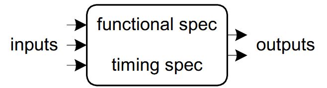
| Extra | <img src="paste-92c3c73e08e660520d9f65d0f54f42a8bf80bc71.jpg"> |
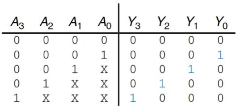
Note 20: ETH::2. Semester::DDCA
Deck: ETH::2. Semester::DDCA
Note Type: Horvath Classic
GUID:
added
Note Type: Horvath Classic
GUID:
GouO^Q1^%L
Previous
Note did not exist
New Note
Front
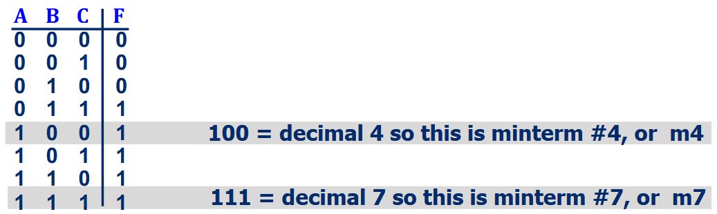
How can the number of a certain minterm be determined without counting lines?
Back
How can the number of a certain minterm be determined without counting lines?
Field-by-field Comparison
| Field | Before | After |
|---|---|---|
| Front | How can the number of a certain minterm be determined without counting lines? | |
| Back | <img src="paste-c687a7cf6e844ba5e3892dff413f47956b4cdd9e.jpg"> |
Note 21: ETH::2. Semester::DDCA
Deck: ETH::2. Semester::DDCA
Note Type: Horvath Cloze
GUID:
added
Note Type: Horvath Cloze
GUID:
GqtZXys=xR
Previous
Note did not exist
New Note
Front
We construct basic logical units out of individual MOS transistors.
These logical units are called logic gates.
These logical units are called logic gates.
Back
We construct basic logical units out of individual MOS transistors.
These logical units are called logic gates.
These logical units are called logic gates.
They implement simple Boolean functions.
Field-by-field Comparison
| Field | Before | After |
|---|---|---|
| Text | We construct basic logical units out of individual MOS transistors. <br><br>These logical units are called {{c1::logic gates}}. | |
| Extra | They implement simple Boolean functions. |
Note 22: ETH::2. Semester::DDCA
Deck: ETH::2. Semester::DDCA
Note Type: Horvath Classic
GUID:
added
Note Type: Horvath Classic
GUID:
H*(W2@+xH+
Previous
Note did not exist
New Note
Front
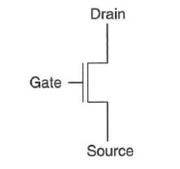
Which type of MOS transistor is this?
Back
Which type of MOS transistor is this?
n-type
Field-by-field Comparison
| Field | Before | After |
|---|---|---|
| Front | Which type of MOS transistor is this?<br><br><img src="paste-7d05867b68f61a963efe3a0b6c769cddefc12b2f.jpg"> | |
| Back | n-type |
Note 23: ETH::2. Semester::DDCA
Deck: ETH::2. Semester::DDCA
Note Type: Horvath Occlusio
GUID:
added
Note Type: Horvath Occlusio
GUID:
HIk47Ngez+
Previous
Note did not exist
New Note
Front
How can we select an address to read?
Back
How can we select an address to read?
Field-by-field Comparison
| Field | Before | After |
|---|---|---|
| Occlusion | {{c1::image-occlusion:rect:left=.0089:top=.5477:width=.2313:height=.092}}<br>{{c2::image-occlusion:rect:left=.0059:top=.8424:width=.7046:height=.1459}}<br> | |
| Image | <img src="paste-cd3e2c310623833536d291253844967607e468c8.jpg"> | |
| Header | How can we select an address to read? |
Note 24: ETH::2. Semester::DDCA
Deck: ETH::2. Semester::DDCA
Note Type: Horvath Classic
GUID:
added
Note Type: Horvath Classic
GUID:
I4o5RfJsK*
Previous
Note did not exist
New Note
Front
How can we build NAND from OR and NOT?
Back
How can we build NAND from OR and NOT?
NAND is equivalent to OR with inputs complemented.
\(B=\overline{(XY)}=\overline X + \overline Y\)
\(B=\overline{(XY)}=\overline X + \overline Y\)
Field-by-field Comparison
| Field | Before | After |
|---|---|---|
| Front | How can we build NAND from OR and NOT? | |
| Back | NAND is equivalent to OR with inputs complemented.<br><br>\(B=\overline{(XY)}=\overline X + \overline Y\)<br><br><img src="paste-7f18a7c0dd30adae86b576c7e3bd558fb91d3c4b.jpg"> |
Note 25: ETH::2. Semester::DDCA
Deck: ETH::2. Semester::DDCA
Note Type: Horvath Classic
GUID:
added
Note Type: Horvath Classic
GUID:
IC[#R`$GWE
Previous
Note did not exist
New Note
Front
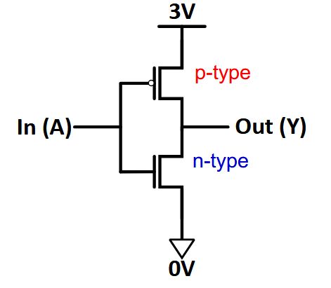
What does this circuit do?
Back
What does this circuit do?
This is the CMOS NOT Gate.
Why do we call it NOT?
Why do we call it NOT?
- If A = 0V then Y = 3V
- If A = 3V then Y = 0V
Field-by-field Comparison
| Field | Before | After |
|---|---|---|
| Front | What does this circuit do?<br><br><img src="paste-1ea8562646d826a66676f32131724f1287dda84a.jpg"> | |
| Back | This is the CMOS NOT Gate.<br><br>Why do we call it NOT?<br><ul><li>If A = 0V then Y = 3V</li><li>If A = 3V then Y = 0V</li></ul> |
Note 26: ETH::2. Semester::DDCA
Deck: ETH::2. Semester::DDCA
Note Type: Horvath Cloze
GUID:
added
Note Type: Horvath Cloze
GUID:
IjnwO_e62-
Previous
Note did not exist
New Note
Front
Pros and Cons of Latches and Flip-Flops:
- Very fast, parallel access
- Very expensive (one bit costs tens of transistors)
Back
Pros and Cons of Latches and Flip-Flops:
- Very fast, parallel access
- Very expensive (one bit costs tens of transistors)
Field-by-field Comparison
| Field | Before | After |
|---|---|---|
| Text | Pros and Cons of Latches and Flip-Flops:<br><ul><li>{{c1::Very fast, parallel access}}</li><li>{{c2::Very expensive (one bit costs tens of transistors)}}</li></ul> |
Note 27: ETH::2. Semester::DDCA
Deck: ETH::2. Semester::DDCA
Note Type: Horvath Classic
GUID:
added
Note Type: Horvath Classic
GUID:
Isdz`E|.1(
Previous
Note did not exist
New Note
Front
Which gate is this?
Back
Which gate is this?
XNOR
Field-by-field Comparison
| Field | Before | After |
|---|---|---|
| Front | Which gate is this?<br><br><img src="paste-09155718b2466228b1738f667e96bcb1c72971dd.jpg"> | |
| Back | XNOR<br><br><img src="paste-262457139ca95f4bd8cd623aa4e060bfe53567df.jpg"> |
Note 28: ETH::2. Semester::DDCA
Deck: ETH::2. Semester::DDCA
Note Type: Horvath Classic
GUID:
added
Note Type: Horvath Classic
GUID:
I{vdVAqb$e
Previous
Note did not exist
New Note
Front
What does FPGA stand for?
Back
What does FPGA stand for?
Field Programmable Gate Array
Field-by-field Comparison
| Field | Before | After |
|---|---|---|
| Front | What does FPGA stand for? | |
| Back | Field Programmable Gate Array |
Note 29: ETH::2. Semester::DDCA
Deck: ETH::2. Semester::DDCA
Note Type: Horvath Cloze
GUID:
added
Note Type: Horvath Cloze
GUID:
J!BC_~c^Tq
Previous
Note did not exist
New Note
Front
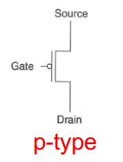
On the p-type transistor, the circuit is closed when the gate is supplied with 0V.
Back
On the p-type transistor, the circuit is closed when the gate is supplied with 0V.
Field-by-field Comparison
| Field | Before | After |
|---|---|---|
| Text | On the p-type transistor, the circuit is closed when the gate is supplied with {{c1::0V}}. | |
| Extra | <img src="paste-283d91233870ed31439a32297a5e66d269bfc534.jpg"> |
Note 30: ETH::2. Semester::DDCA
Deck: ETH::2. Semester::DDCA
Note Type: Horvath Classic
GUID:
added
Note Type: Horvath Classic
GUID:
J!Fb=eJD*B
Previous
Note did not exist
New Note
Front
Addressability?
Back
Addressability?
3-bits
Field-by-field Comparison
| Field | Before | After |
|---|---|---|
| Front | Addressability?<br><br><img src="paste-adeed554f607d7f9c2ae3a806f83b02c89cef624.jpg"> | |
| Back | 3-bits |
Note 31: ETH::2. Semester::DDCA
Deck: ETH::2. Semester::DDCA
Note Type: Horvath Cloze
GUID:
added
Note Type: Horvath Cloze
GUID:
J$BvIDQ[e=
Previous
Note did not exist
New Note
Front
If the gate of an n-type transistor is supplied with a high voltage, the connection from source to drain acts like a piece of wire (i.e., the circuit is closed).
Back
If the gate of an n-type transistor is supplied with a high voltage, the connection from source to drain acts like a piece of wire (i.e., the circuit is closed).
Depending on the technology, high voltage can range from 0.3V to 3V.
Field-by-field Comparison
| Field | Before | After |
|---|---|---|
| Text | If the gate of an n-type transistor is supplied with {{c1::a high}} voltage, the connection from source to drain acts like {{c2::a piece of wire (i.e., the circuit is closed)}}. | |
| Extra | Depending on the technology, high voltage can range from 0.3V to 3V. |
Note 32: ETH::2. Semester::DDCA
Deck: ETH::2. Semester::DDCA
Note Type: Horvath Classic
GUID:
added
Note Type: Horvath Classic
GUID:
JWeqr#]4c
Previous
Note did not exist
New Note
Front
How can we convert from the Minterm expansion of \(F\) to the Maxterm expansion of \(\overline F\)?
Back
How can we convert from the Minterm expansion of \(F\) to the Maxterm expansion of \(\overline F\)?
Rewrite in Maxterm form, using the same indices as \(F\).
\[\begin{array}{r l c r l} \text{E.g., } F(A,B,C) & = \sum m(3,4,5,6,7) & \longrightarrow & \overline{F}(A,B,C) & = \prod M(3,4,5,6,7) \\ & = \prod M(0,1,2) & \longrightarrow & & = \sum m(0,1,2) \end{array}\]
\[\begin{array}{r l c r l} \text{E.g., } F(A,B,C) & = \sum m(3,4,5,6,7) & \longrightarrow & \overline{F}(A,B,C) & = \prod M(3,4,5,6,7) \\ & = \prod M(0,1,2) & \longrightarrow & & = \sum m(0,1,2) \end{array}\]
Field-by-field Comparison
| Field | Before | After |
|---|---|---|
| Front | How can we convert from the Minterm expansion of \(F\) to the Maxterm expansion of \(\overline F\)? | |
| Back | Rewrite in Maxterm form, using the same indices as \(F\).<br>\[\begin{array}{r l c r l} \text{E.g., } F(A,B,C) & = \sum m(3,4,5,6,7) & \longrightarrow & \overline{F}(A,B,C) & = \prod M(3,4,5,6,7) \\ & = \prod M(0,1,2) & \longrightarrow & & = \sum m(0,1,2) \end{array}\]<br> |
Note 33: ETH::2. Semester::DDCA
Deck: ETH::2. Semester::DDCA
Note Type: Horvath Classic
GUID:
added
Note Type: Horvath Classic
GUID:
J}Cp1R>RJL
Previous
Note did not exist
New Note
Front
What is this functionally?
Back
What is this functionally?
A memory-based lookup table.
Field-by-field Comparison
| Field | Before | After |
|---|---|---|
| Front | What is this functionally?<br><br><img src="paste-da1444290ceb76a444f3cae190bb00d91cbf15ff.jpg"> | |
| Back | A memory-based lookup table. |
Note 34: ETH::2. Semester::DDCA
Deck: ETH::2. Semester::DDCA
Note Type: Horvath Classic
GUID:
added
Note Type: Horvath Classic
GUID:
KEEa>PCXE`
Previous
Note did not exist
New Note
Front
What's the formula for energy consumption?
Back
What's the formula for energy consumption?
Power * Time
Field-by-field Comparison
| Field | Before | After |
|---|---|---|
| Front | What's the formula for energy consumption? | |
| Back | Power * Time |
Note 35: ETH::2. Semester::DDCA
Deck: ETH::2. Semester::DDCA
Note Type: Horvath Cloze
GUID:
added
Note Type: Horvath Cloze
GUID:
L)2IfSjkLM
Previous
Note did not exist
New Note
Front
On the n-type transistor, the circuit is closed when the gate is supplied with 3V.
Back
On the n-type transistor, the circuit is closed when the gate is supplied with 3V.
Field-by-field Comparison
| Field | Before | After |
|---|---|---|
| Text | On the n-type transistor, the circuit is closed when the gate is supplied with {{c1::3V}}. | |
| Extra | <img src="paste-58a159d5191f269f58343aa3187998262875b89e.jpg"> |
Note 36: ETH::2. Semester::DDCA
Deck: ETH::2. Semester::DDCA
Note Type: Horvath Classic
GUID:
added
Note Type: Horvath Classic
GUID:
Lk!m/FJd3!
Previous
Note did not exist
New Note
Front
How can we convert from Maxterm to Minterm?
Back
How can we convert from Maxterm to Minterm?
- Rewrite maxterm shorthand using minterm shorthand
- Replace maxterm indices with the indices not already used
Field-by-field Comparison
| Field | Before | After |
|---|---|---|
| Front | How can we convert from Maxterm to Minterm? | |
| Back | <ol><li>Rewrite maxterm shorthand using minterm shorthand</li><li>Replace maxterm indices with the indices not already used<br></li></ol>E.g., \(F(A,B,C) = \prod M(0,1,2) = \sum m(3,4,5,6,7)\) |
Note 37: ETH::2. Semester::DDCA
Deck: ETH::2. Semester::DDCA
Note Type: Horvath Cloze
GUID:
added
Note Type: Horvath Cloze
GUID:
Lyr2I#>S6v
Previous
Note did not exist
New Note
Front
Decoders can be combined with OR gates to build logic functions.
Back
Decoders can be combined with OR gates to build logic functions.
Field-by-field Comparison
| Field | Before | After |
|---|---|---|
| Text | Decoders can be combined with {{c1::OR gates}} to build logic functions. | |
| Extra | <img src="paste-4b9926a6c0a612f21c80818ed3d3a9b2c1965b52.jpg"> |
Note 38: ETH::2. Semester::DDCA
Deck: ETH::2. Semester::DDCA
Note Type: Horvath Cloze
GUID:
added
Note Type: Horvath Cloze
GUID:
MH2*~,1ehe
Previous
Note did not exist
New Note
Front
\(X \bullet Y + X \bullet \overline{Y} = X\)
Back
\(X \bullet Y + X \bullet \overline{Y} = X\)
Field-by-field Comparison
| Field | Before | After |
|---|---|---|
| Text | \(X \bullet Y + X \bullet \overline{Y} = {{c1::X}}\) |
Note 39: ETH::2. Semester::DDCA
Deck: ETH::2. Semester::DDCA
Note Type: Horvath Classic
GUID:
added
Note Type: Horvath Classic
GUID:
MWmGMTiH]o
Previous
Note did not exist
New Note
Front
What is an implicant?
Back
What is an implicant?
A product (AND) of literals.
\((A \cdot B \cdot \overline{C}) \text{ , } (\overline{A} \cdot C) \text{ , } (B \cdot \overline{C})\)
\((A \cdot B \cdot \overline{C}) \text{ , } (\overline{A} \cdot C) \text{ , } (B \cdot \overline{C})\)
Field-by-field Comparison
| Field | Before | After |
|---|---|---|
| Front | What is an implicant? | |
| Back | A product (AND) of literals.<br><br>\((A \cdot B \cdot \overline{C}) \text{ , } (\overline{A} \cdot C) \text{ , } (B \cdot \overline{C})\) |
Note 40: ETH::2. Semester::DDCA
Deck: ETH::2. Semester::DDCA
Note Type: Horvath Classic
GUID:
added
Note Type: Horvath Classic
GUID:
MZTQ<6vlZH
Previous
Note did not exist
New Note
Front
What do the X's here mean?
Back
What do the X's here mean?
X (Don't Care) means I don't care what the value of this input is.
Field-by-field Comparison
| Field | Before | After |
|---|---|---|
| Front | What do the X's here mean?<br><br><img src="paste-9e8019103c346073b358f3b23b79416178cdc519.jpg"> | |
| Back | X (Don't Care) means I don't care what the value of this input is. |
Note 41: ETH::2. Semester::DDCA
Deck: ETH::2. Semester::DDCA
Note Type: Horvath Cloze
GUID:
added
Note Type: Horvath Cloze
GUID:
M{Tz&Xi?.~
Previous
Note did not exist
New Note
Front
Every unique location in memory is indexed with a unique address.
Back
Every unique location in memory is indexed with a unique address.
4 locations require 2 address bits (log[#locations]).
Field-by-field Comparison
| Field | Before | After |
|---|---|---|
| Text | Every unique location in memory is indexed with a unique {{c1::address}}. | |
| Extra | 4 locations require 2 address bits (log[#locations]). |
Note 42: ETH::2. Semester::DDCA
Deck: ETH::2. Semester::DDCA
Note Type: Horvath Cloze
GUID:
added
Note Type: Horvath Cloze
GUID:
N*9Rha0FR,
Previous
Note did not exist
New Note
Front
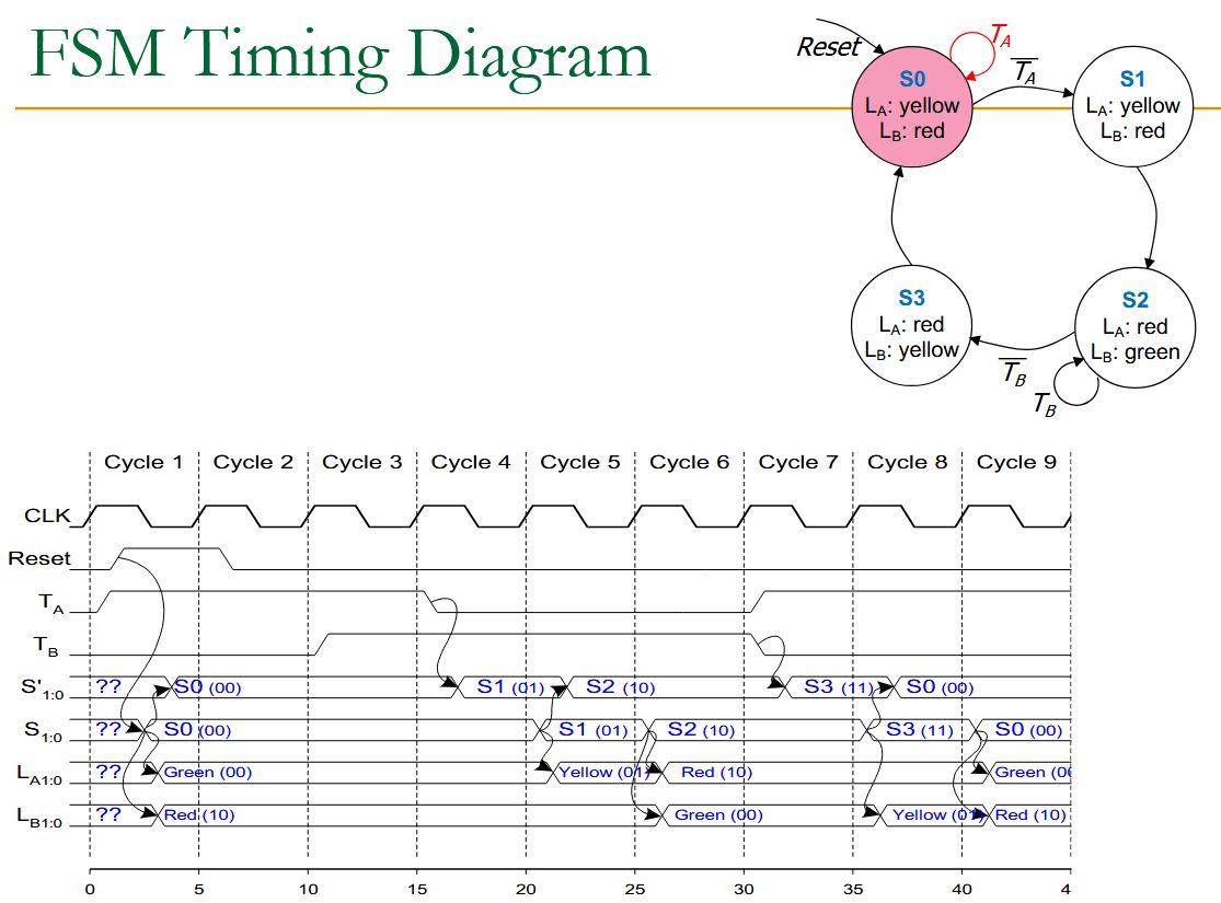
Each FSM consists of three separate parts:
- next state logic
- state register
- output logic
Back
Each FSM consists of three separate parts:
- next state logic
- state register
- output logic
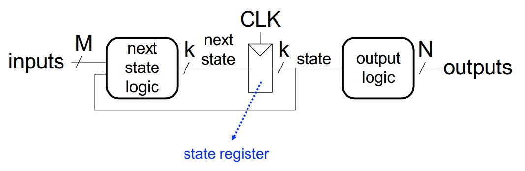
At the beginning of the clock cycle, next state is latched into the state register
Field-by-field Comparison
| Field | Before | After |
|---|---|---|
| Text | Each FSM consists of three separate parts:<br><ol><li>{{c1::next state logic}}</li><li>{{c2::state register}}</li><li>{{c3::output logic}}</li></ol> | |
| Extra | <img src="paste-f282a35cb1ef5e0d4f8f098548b2bdb621bdf0da.jpg"><br><br>At the beginning of the clock cycle, next state is latched into the state register |
Note 43: ETH::2. Semester::DDCA
Deck: ETH::2. Semester::DDCA
Note Type: Horvath Classic
GUID:
added
Note Type: Horvath Classic
GUID:
NO,[UqkjjY
Previous
Note did not exist
New Note
Front
Address space size?
Back
Address space size?
2 (total of 6 bits)
Field-by-field Comparison
| Field | Before | After |
|---|---|---|
| Front | Address space size?<br><br><img src="paste-adeed554f607d7f9c2ae3a806f83b02c89cef624.jpg"> | |
| Back | 2 (total of 6 bits) |
Note 44: ETH::2. Semester::DDCA
Deck: ETH::2. Semester::DDCA
Note Type: Horvath Cloze
GUID:
added
Note Type: Horvath Cloze
GUID:
Nr/WO;(0{4
Previous
Note did not exist
New Note
Front
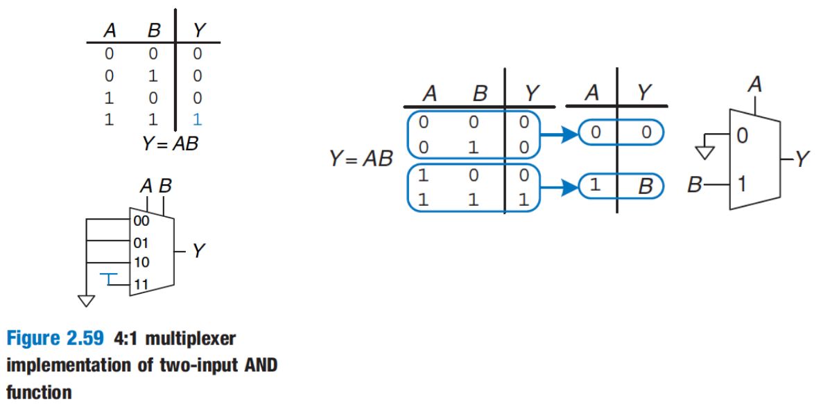
Multiplexers can be used as "lookup tables" to perform logic functions.
Back
Multiplexers can be used as "lookup tables" to perform logic functions.
Field-by-field Comparison
| Field | Before | After |
|---|---|---|
| Text | Multiplexers can be used as {{c1::"lookup tables" to perform logic functions}}. | |
| Extra | <img src="paste-a0643b754113ab32abc6e5adfed855ac37f050e3.jpg"> |
Note 45: ETH::2. Semester::DDCA
Deck: ETH::2. Semester::DDCA
Note Type: Horvath Classic
GUID:
added
Note Type: Horvath Classic
GUID:
P2t5@m8Q~.
Previous
Note did not exist
New Note
Front
What gate is this?
Back
What gate is this?
This is the CMOS AND Gate.
Field-by-field Comparison
| Field | Before | After |
|---|---|---|
| Front | What gate is this?<br><br><img src="paste-2ad6d40fa1eb42fa0ccdeb5a2af1449399f4157c.jpg"> | |
| Back | This is the CMOS AND Gate.<br><br><img src="paste-3ec26993d5dc59b7a394208bdd22963894227581.jpg"> |
Note 46: ETH::2. Semester::DDCA
Deck: ETH::2. Semester::DDCA
Note Type: Horvath Cloze
GUID:
added
Note Type: Horvath Cloze
GUID:
P938wRh{~H
Previous
Note did not exist
New Note
Front
Which properties do we need to implement a state register?
- We need to store data at the beginning of every clock cycle
- The data must be available during the entire clock cycle
Back
Which properties do we need to implement a state register?
- We need to store data at the beginning of every clock cycle
- The data must be available during the entire clock cycle
Field-by-field Comparison
| Field | Before | After |
|---|---|---|
| Text | Which properties do we need to implement a state register?<br><ol><li>{{c1::We need to store data at the beginning of every clock cycle}}<br></li><li>{{c2::The data must be available during the entire clock cycle}}<br></li></ol> | |
| Extra | <img src="paste-d15605117cc9664c84a7753d40f0a3d09f3febbd.jpg"><br><img src="paste-f6afd0db6d1e758d9b809052a6b2ad201b0950b0.jpg"> |
Note 47: ETH::2. Semester::DDCA
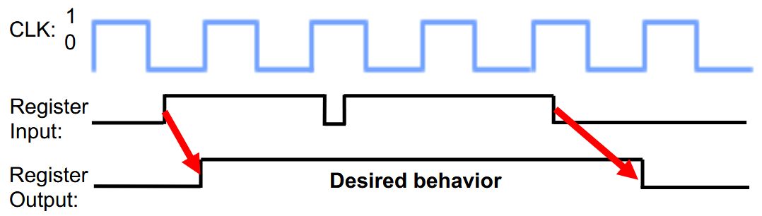
Deck: ETH::2. Semester::DDCA
Note Type: Horvath Cloze
GUID:
added
Note Type: Horvath Cloze
GUID:
PMc1ViG{^J
Previous
Note did not exist
New Note
Front
Most modern computers are synchronous "machines".
Back
Most modern computers are synchronous "machines".
State transitions take place at fixed units of time (i.e., potentially delayed response to input, synchronized to an external signal).
Controlled in part by a clock, as we will see soon.
Controlled in part by a clock, as we will see soon.
Field-by-field Comparison
| Field | Before | After |
|---|---|---|
| Text | Most modern computers are {{c1::synchronous}} "machines". | |
| Extra | State transitions take place at fixed units of time (i.e., potentially delayed response to input, synchronized to an external signal).<br><br>Controlled in part by a clock, as we will see soon. |
Note 48: ETH::2. Semester::DDCA
Deck: ETH::2. Semester::DDCA
Note Type: Horvath Cloze
GUID:
added
Note Type: Horvath Cloze
GUID:
Q+Ol+3O^DB
Previous
Note did not exist
New Note
Front
Series connections are slower than parallel connections.
Back
Series connections are slower than parallel connections.
More resistance on the wire.
Field-by-field Comparison
| Field | Before | After |
|---|---|---|
| Text | Series connections are {{c1::slower::Speed}} than parallel connections. | |
| Extra | More resistance on the wire. |
Note 49: ETH::2. Semester::DDCA
Deck: ETH::2. Semester::DDCA
Note Type: Horvath Cloze
GUID:
added
Note Type: Horvath Cloze
GUID:
QSB?1}FgZ9
Previous
Note did not exist
New Note
Front
p-type transistors are good at pulling up the voltage.
Back
p-type transistors are good at pulling up the voltage.
Field-by-field Comparison
| Field | Before | After |
|---|---|---|
| Text | <b>p</b>-type transistors are good at pulling {{c1::u<b>p</b>}} the voltage. |
Note 50: ETH::2. Semester::DDCA
Deck: ETH::2. Semester::DDCA
Note Type: Horvath Occlusio
GUID:
added
Note Type: Horvath Occlusio
GUID:
[,YWN{Lwu
Previous
Note did not exist
New Note
Front
What is this?
Back
What is this?
Field-by-field Comparison
| Field | Before | After |
|---|---|---|
| Image | <img src="paste-6a8326151aeedf40c81bab85eb67ee61a0bfdc28.jpg"> | |
| Header | What is this? |
Note 51: ETH::2. Semester::DDCA
Deck: ETH::2. Semester::DDCA
Note Type: Horvath Classic
GUID:
added
Note Type: Horvath Classic
GUID:
b]5EOR.;[y
Previous
Note did not exist
New Note
Front
What is a Finite State Machine (FSM)?
Back
What is a Finite State Machine (FSM)?
A discrete-time model of a stateful system.
Each state represents a snapshot of the system at a given time.
Each state represents a snapshot of the system at a given time.
Field-by-field Comparison
| Field | Before | After |
|---|---|---|
| Front | What is a Finite State Machine (FSM)? | |
| Back | A discrete-time model of a stateful system.<br><br>Each state represents a snapshot of the system at a given time. |
Note 52: ETH::2. Semester::DDCA
Deck: ETH::2. Semester::DDCA
Note Type: Horvath Classic
GUID:
added
Note Type: Horvath Classic
GUID:
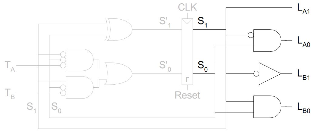
c.C#J,&->z
Previous
Note did not exist
New Note
Front
What is the non-greyed out part of the circuit?
Back
What is the non-greyed out part of the circuit?
Output logic and outputs.
Field-by-field Comparison
| Field | Before | After |
|---|---|---|
| Front | What is the non-greyed out part of the circuit?<br><br><img src="paste-e862550d817fcb452eefec1d1adda5fe368464f1.jpg"> | |
| Back | Output logic and outputs.<br><br><img src="paste-cd6ef59f2ccfee5f7ab46a1cdc992280c12a7ba5.jpg"> |
Note 53: ETH::2. Semester::DDCA
Deck: ETH::2. Semester::DDCA
Note Type: Horvath Classic
GUID:
added
Note Type: Horvath Classic
GUID:
c>-yp[Ry[S
Previous
Note did not exist
New Note
Front
How can we make an AND gate?
Back
How can we make an AND gate?
We make an AND gate using one NAND gate and one NOT gate:
Field-by-field Comparison
| Field | Before | After |
|---|---|---|
| Front | How can we make an AND gate? | |
| Back | We make an AND gate using one NAND gate and one NOT gate:<br><br><img src="paste-0596c472398ba477eff721024a309ad41e750430.jpg"> |
Note 54: ETH::2. Semester::DDCA
Deck: ETH::2. Semester::DDCA
Note Type: Horvath Occlusio
GUID:
added
Note Type: Horvath Occlusio
GUID:
cK)3)DLM_o
Previous
Note did not exist
New Note
Front
Full Adder
Back
Full Adder
Field-by-field Comparison
| Field | Before | After |
|---|---|---|
| Occlusion | {{c1::image-occlusion:rect:left=.8168:top=.9307:width=.1774:height=.0558:oi=1}}<br> | |
| Image | <img src="paste-8436c8f8af1bf260ebd78993c1d11a17c97c0dd2.jpg"> | |
| Header | Full Adder |
Note 55: ETH::2. Semester::DDCA
Deck: ETH::2. Semester::DDCA
Note Type: Horvath Cloze
GUID:
added
Note Type: Horvath Cloze
GUID:
cRGP4XGmZM
Previous
Note did not exist
New Note
Front
Product of Sums is equivalent to CNF.
Back
Product of Sums is equivalent to CNF.
This is also the DeMorgan of SOP of \(\overline F\).
Field-by-field Comparison
| Field | Before | After |
|---|---|---|
| Text | Product of Sums is equivalent to {{c1::CNF}}. | |
| Extra | This is also the DeMorgan of SOP of \(\overline F\). |
Note 56: ETH::2. Semester::DDCA
Deck: ETH::2. Semester::DDCA
Note Type: Horvath Classic
GUID:
added
Note Type: Horvath Classic
GUID:
e.w!.^HZQk
Previous
Note did not exist
New Note
Front
What is this?
Back
What is this?
An equality checker.
Field-by-field Comparison
| Field | Before | After |
|---|---|---|
| Front | What is this?<br><br><img src="paste-9ee9299a0aa47519e61e8ffe9cefcd2d2ffa51c2.jpg"> | |
| Back | An equality checker. |
Note 57: ETH::2. Semester::DDCA
Deck: ETH::2. Semester::DDCA
Note Type: Horvath Classic
GUID:
added
Note Type: Horvath Classic
GUID:
e1dy/}l($w
Previous
Note did not exist
New Note
Front
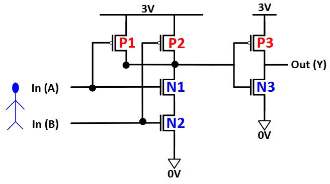
What does this circuit do?
Back
What does this circuit do?
It's the CMOS NAND Gate.
- P1 and P2 are in parallel; only one must be ON to pull up the output to 3V.
- N1 and N2 are connected in series; both must be ON to pull down the output to 0V.
Field-by-field Comparison
| Field | Before | After |
|---|---|---|
| Front | What does this circuit do?<br><br><img src="paste-bccbffeadc7963887cae6412e8d018f79008f8a4.jpg"> | |
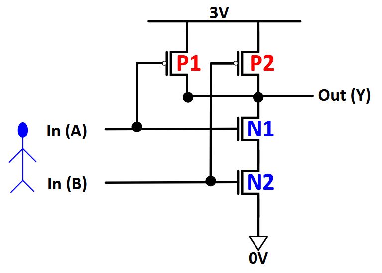
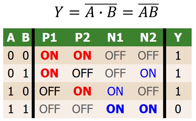
| Back | It's the CMOS NAND Gate.<br><br><img src="paste-cc6b665cdbfe3838f2f72c3f5c383b6787057523.jpg"><br><div><ul><li>P1 and P2 are <b>in parallel</b>; only one must be ON to pull up the output to 3V.</li><li>N1 and N2 are connected <b>in series</b>; both must be ON to pull down the output to 0V.</li></ul></div> |
Note 58: ETH::2. Semester::DDCA
Deck: ETH::2. Semester::DDCA
Note Type: Horvath Classic
GUID:
added
Note Type: Horvath Classic
GUID:
eh2^a;u=sR
Previous
Note did not exist
New Note
Front
How can we convert the expansion of \(F\) to the expansion of \(\overline F\)?
Back
How can we convert the expansion of \(F\) to the expansion of \(\overline F\)?
\[\begin{array}{r l c r l}
\text{E.g., } F(A,B,C) & = \sum m(3,4,5,6,7) & \longrightarrow & \overline{F}(A,B,C) & = \sum m(0,1,2) \\
& = \prod M(0,1,2) & \longrightarrow & & = \prod M(3,4,5,6,7)
\end{array}\]
Field-by-field Comparison
| Field | Before | After |
|---|---|---|
| Front | How can we convert the expansion of \(F\) to the expansion of \(\overline F\)? | |
| Back | \[\begin{array}{r l c r l} \text{E.g., } F(A,B,C) & = \sum m(3,4,5,6,7) & \longrightarrow & \overline{F}(A,B,C) & = \sum m(0,1,2) \\ & = \prod M(0,1,2) & \longrightarrow & & = \prod M(3,4,5,6,7) \end{array}\]<br> |
Note 59: ETH::2. Semester::DDCA
Deck: ETH::2. Semester::DDCA
Note Type: Horvath Cloze
GUID:
added
Note Type: Horvath Cloze
GUID:
fj@3y5gt5P
Previous
Note did not exist
New Note
Front
The state of a system is a snapshot of all relevant elements of the system at the moment of the snapshot.
Back
The state of a system is a snapshot of all relevant elements of the system at the moment of the snapshot.
Field-by-field Comparison
| Field | Before | After |
|---|---|---|
| Text | The {{c1::state}} of a system is a snapshot of all relevant elements of the system at the moment of the snapshot. |
Note 60: ETH::2. Semester::DDCA
Deck: ETH::2. Semester::DDCA
Note Type: Horvath Occlusio
GUID:
added
Note Type: Horvath Occlusio
GUID:
g(oknS2XIO
Previous
Note did not exist
New Note
Front
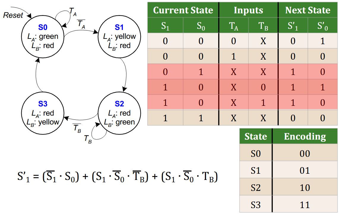
Determine the SOP of \(S_1'\) from this state transition table:
Back
Determine the SOP of \(S_1'\) from this state transition table:
Field-by-field Comparison
| Field | Before | After |
|---|---|---|
| Occlusion | {{c1::image-occlusion:rect:left=.1192:top=.7777:width=.5322:height=.0901:oi=1}}<br> | |
| Image | <img src="paste-2b0785e36a987370d617f3eeadb768dc3c9ce66d.jpg"> | |
| Header | Determine the SOP of \(S_1'\) from this state transition table: |
Note 61: ETH::2. Semester::DDCA
Deck: ETH::2. Semester::DDCA
Note Type: Horvath Classic
GUID:
added
Note Type: Horvath Classic
GUID:
g-~*^Ki!(:
Previous
Note did not exist
New Note
Front
How do we model a BUS as a circuit?
Back
How do we model a BUS as a circuit?
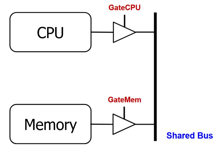
You can have two tri-state buffers: one driven by CPU, the other memory; and ensure at most one is enabled at any time.
Field-by-field Comparison
| Field | Before | After |
|---|---|---|
| Front | How do we model a BUS as a circuit? | |
| Back | You can have two tri-state buffers: one driven by CPU, the other memory; and ensure at most one is enabled at any time.<br><br><img src="paste-3e60268fdf3d3d4e9613807017fd11ee2dd4909f.jpg"> |
Note 62: ETH::2. Semester::DDCA
Deck: ETH::2. Semester::DDCA
Note Type: Horvath Classic
GUID:
added
Note Type: Horvath Classic
GUID:
g.dcXCwTR^
Previous
Note did not exist
New Note
Front
How many locations and bits does this memory array have?
Back
How many locations and bits does this memory array have?
4 locations X 3 bits
Field-by-field Comparison
| Field | Before | After |
|---|---|---|
| Front | How many locations and bits does this memory array have?<br><br><img src="paste-527c14fba71cb77a30a80a0db3ff30a5ca8a1b03.jpg"> | |
| Back | 4 locations X 3 bits |
Note 63: ETH::2. Semester::DDCA
Deck: ETH::2. Semester::DDCA
Note Type: Horvath Classic
GUID:
added
Note Type: Horvath Classic
GUID:
g8HHZjvwjk
Previous
Note did not exist
New Note
Front
How do we guarantee correct operation of an R-S Latch?
Back
How do we guarantee correct operation of an R-S Latch?
We add two more NAND gates.
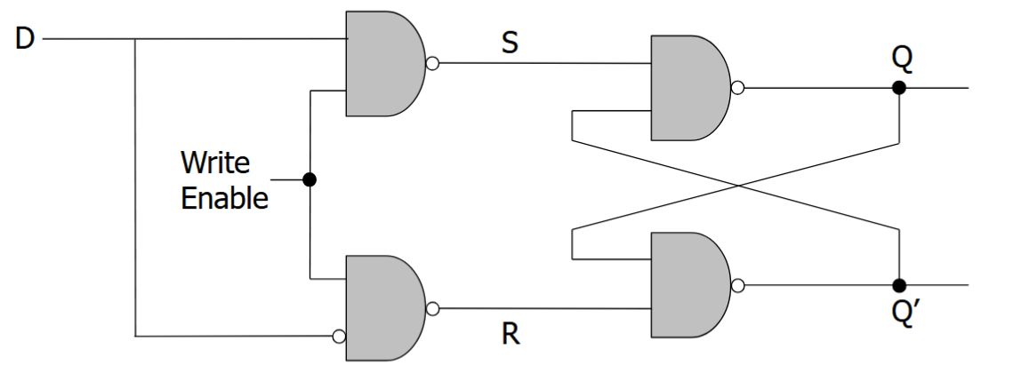
\(Q\) takes the value of \(D\), when write enable (WE) is set to 1.
\(S\) and \(R\) can never be 0 at the same time!
\(Q\) takes the value of \(D\), when write enable (WE) is set to 1.
\(S\) and \(R\) can never be 0 at the same time!
Field-by-field Comparison
| Field | Before | After |
|---|---|---|
| Front | How do we guarantee correct operation of an R-S Latch? | |
| Back | We add two more NAND gates.<br><br><img src="paste-75ed2b046c6dd5698e1016b588d9baa5ff3affdf.jpg"><br><br>\(Q\) takes the value of \(D\), when write enable (WE) is set to 1.<br>\(S\) and \(R\) can never be 0 at the same time!<br><br><img src="paste-d6a38ff36eeae6a05033cd1da3fa1f32da25717f.jpg"> |
Note 64: ETH::2. Semester::DDCA
Deck: ETH::2. Semester::DDCA
Note Type: Horvath Cloze
GUID:
added
Note Type: Horvath Cloze
GUID:
g<38ETccf&
Previous
Note did not exist
New Note
Front
Combinational logic evaluates for the length of the clock cycle.
Back
Combinational logic evaluates for the length of the clock cycle.
Field-by-field Comparison
| Field | Before | After |
|---|---|---|
| Text | Combinational logic evaluates for the {{c1::length}} of the clock cycle. |
Note 65: ETH::2. Semester::DDCA
Deck: ETH::2. Semester::DDCA
Note Type: Horvath Classic
GUID:
added
Note Type: Horvath Classic
GUID:
h!H8&>iQx{
Previous
Note did not exist
New Note
Front
How do we determine the number of OR gates in a PLA?
Back
How do we determine the number of OR gates in a PLA?
The number of output columns in the truth table.
Field-by-field Comparison
| Field | Before | After |
|---|---|---|
| Front | How do we determine the number of OR gates in a PLA? | |
| Back | The number of output columns in the truth table. |
Note 66: ETH::2. Semester::DDCA
Deck: ETH::2. Semester::DDCA
Note Type: Horvath Classic
GUID:
added
Note Type: Horvath Classic
GUID:
hQ)3[a]Xq<
Previous
Note did not exist
New Note
Front
What gates is this?
Back
What gates is this?
The CMOS NAND Gate.
Field-by-field Comparison
| Field | Before | After |
|---|---|---|
| Front | What gates is this?<br><br><img src="paste-b6777165efef100cab46f26906ce60b1d5d3a866.jpg"> | |
| Back | The CMOS NAND Gate.<br><br><img src="paste-953f00465848000258867b4eb3678f8b985d22d1.jpg"> |
Note 67: ETH::2. Semester::DDCA
Deck: ETH::2. Semester::DDCA
Note Type: Horvath Classic
GUID:
added
Note Type: Horvath Classic
GUID:
iyge$&[U#_
Previous
Note did not exist
New Note
Front
What is this?
Back
What is this?
A priority circuit.
- Inputs: "Requestors" with priority levels
- Outputs: "Grant" signal for each requestor
Field-by-field Comparison
| Field | Before | After |
|---|---|---|
| Front | What is this?<br><br><img src="paste-50fbc0b6a9081d2f896cc292f56cc4a470bd44ab.jpg"> | |
| Back | A priority circuit.<br><ul><li>Inputs: "Requestors" with priority levels</li><li>Outputs: "Grant" signal for each requestor</li></ul> |
Note 68: ETH::2. Semester::DDCA
Deck: ETH::2. Semester::DDCA
Note Type: Horvath Cloze
GUID:
added
Note Type: Horvath Cloze
GUID:
jY?vAb-}P$
Previous
Note did not exist
New Note
Front
Pros and cons of other storage technology (flash memory, hard disk, tape)
- Very cheap
- Much slower, access takes a long time, non-volatile
Back
Pros and cons of other storage technology (flash memory, hard disk, tape)
- Very cheap
- Much slower, access takes a long time, non-volatile
Field-by-field Comparison
| Field | Before | After |
|---|---|---|
| Text | Pros and cons of other storage technology (flash memory, hard disk, tape)<br><ul><li>{{c1::Very cheap}}</li><li>{{c2::Much slower, access takes a long time, non-volatile}}</li></ul> |
Note 69: ETH::2. Semester::DDCA
Deck: ETH::2. Semester::DDCA
Note Type: Horvath Cloze
GUID:
added
Note Type: Horvath Cloze
GUID:
jgnr@Obi8f
Previous
Note did not exist
New Note
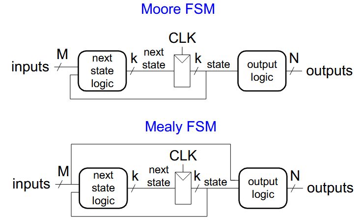
Front
Two types of finite state machines differ in the output logic:
- Moore FSM: outputs depend only on the current state
- Mealy FSM: outputs depend on the current state and the inputs
Back
Two types of finite state machines differ in the output logic:
- Moore FSM: outputs depend only on the current state
- Mealy FSM: outputs depend on the current state and the inputs
Field-by-field Comparison
| Field | Before | After |
|---|---|---|
| Text | Two types of finite state machines differ in the output logic:<br><ol><li>{{c1::Moore FSM}}: outputs depend only on the current state</li><li>{{c1::Mealy FSM}}: outputs depend on the current state and the inputs</li></ol> | |
| Extra | <img src="paste-8c32ce33990f4253676703e6ef1745ff9f544c8e.jpg"> |
Note 70: ETH::2. Semester::DDCA
Deck: ETH::2. Semester::DDCA
Note Type: Horvath Cloze
GUID:
added
Note Type: Horvath Cloze
GUID:
jylgnWO`cY
Previous
Note did not exist
New Note
Front
If both networks are ON at the same time, there is a short circuit → likely incorrect operation.
Back
If both networks are ON at the same time, there is a short circuit → likely incorrect operation.
Field-by-field Comparison
| Field | Before | After |
|---|---|---|
| Text | <img src="paste-a3eb18d4f8b16544780bf296d94ae3cb0386642d.jpg"><br><br><div>If both networks are ON at the same time, there is {{c1::a <strong>short circuit</strong> → likely incorrect operation}}.</div> |
Note 71: ETH::2. Semester::DDCA
Deck: ETH::2. Semester::DDCA
Note Type: Horvath Classic
GUID:
added
Note Type: Horvath Classic
GUID:
kOBb
Previous
Note did not exist
New Note
Front
What does the Z mean here?
Back
What does the Z mean here?
Signal that is not driven by any circuit (e.g. open circuit, floating wire).
Field-by-field Comparison
| Field | Before | After |
|---|---|---|
| Front | What does the Z mean here?<br><br><img src="paste-6aad4a37bc003259212e2f00d56e604b0cf5c2b8.jpg"> | |
| Back | Signal that is not driven by any circuit (e.g. open circuit, floating wire). |
Note 72: ETH::2. Semester::DDCA
Deck: ETH::2. Semester::DDCA
Note Type: Horvath Cloze
GUID:
added
Note Type: Horvath Cloze
GUID:
kjuyg1m}9]
Previous
Note did not exist
New Note
Front
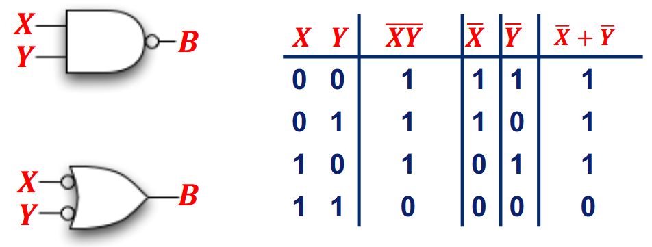
\(A+B\) signifies "A or B".
Back
\(A+B\) signifies "A or B".
Field-by-field Comparison
| Field | Before | After |
|---|---|---|
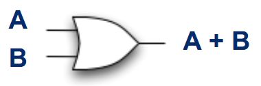
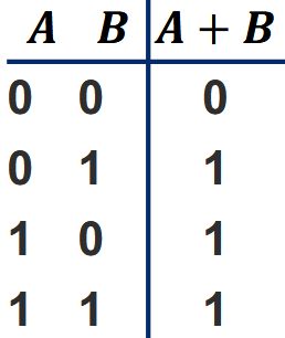
| Text | \(A+B\) signifies {{c1::"A or B"}}. | |
| Extra | <img src="paste-e9d93adb6e4be16c829b5ca7bc0873cb10bfaaad.jpg"><br><img src="paste-98398b7664b21c58363c0b63982187f6bc6981aa.jpg"> |
Note 73: ETH::2. Semester::DDCA
Deck: ETH::2. Semester::DDCA
Note Type: Horvath Cloze
GUID:
added
Note Type: Horvath Cloze
GUID:
km!Z
Previous
Note did not exist
New Note
Front
One-Hot Encoding:
- Each bit encodes a different state
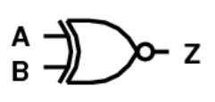
- Uses num_states bits to represent the states
- Exactly 1 bit is "hot" for a given state
- Simplest design process – very automatable
- Minimizes next state logic, maximizes # flip-flops
Back
One-Hot Encoding:
- Each bit encodes a different state
- Uses num_states bits to represent the states
- Exactly 1 bit is "hot" for a given state
- Simplest design process – very automatable
- Minimizes next state logic, maximizes # flip-flops
Example state encodings: 0001, 0010, 0100, 1000
Field-by-field Comparison
| Field | Before | After |
|---|---|---|
| Text | <div>{{c1::One-Hot Encoding}}<strong>:</strong></div> <ul> <li>Each bit {{c4::encodes a different state <ul> <li>Uses <em>num_states</em> bits to represent the states</li> <li>Exactly 1 bit is "hot" for a given state</li></ul>}}</li> <li><strong>Simplest design process</strong> – very automatable</li> <li><strong>Minimizes</strong> {{c2::next state logic}}, <strong>maximizes</strong> {{c3::# flip-flops}}</li></ul> | |
| Extra | <em>Example state encodings:</em> 0001, 0010, 0100, 1000 |
Note 74: ETH::2. Semester::DDCA
Deck: ETH::2. Semester::DDCA
Note Type: Horvath Classic
GUID:
added
Note Type: Horvath Classic
GUID:
kp|/N}vt~s
Previous
Note did not exist
New Note
Front
How do we determine the number of AND gates in a PLA?
Back
How do we determine the number of AND gates in a PLA?
For an n-input logic function, we need a PLA with 2ⁿ n-input AND gates.
Remember SOP: the number of possible minterms
Remember SOP: the number of possible minterms
Field-by-field Comparison
| Field | Before | After |
|---|---|---|
| Front | <div><strong>How do we determine the number of AND gates in a PLA?</strong></div> | |
| Back | For an n-input logic function, we need a PLA with 2ⁿ n-input AND gates.<br><strong><br>Remember SOP:</strong> the number of possible minterms |
Note 75: ETH::2. Semester::DDCA
Deck: ETH::2. Semester::DDCA
Note Type: Horvath Occlusio
GUID:
added
Note Type: Horvath Occlusio
GUID:
l:)hd01;==
Previous
Note did not exist
New Note
Front
What is this hidden component?
Back
What is this hidden component?
Field-by-field Comparison
| Field | Before | After |
|---|---|---|
| Occlusion | {{c1::image-occlusion:rect:left=.3893:top=.0178:width=.4877:height=.0674:oi=1}}<br>{{c2::image-occlusion:rect:left=.5552:top=.3107:width=.4354:height=.1021:oi=1}}<br> | |
| Image | <img src="paste-bc35d0ae17174e4109a0bc070e1da9b4d468886b.jpg"> | |
| Header | What is this hidden component? |
Note 76: ETH::2. Semester::DDCA
Deck: ETH::2. Semester::DDCA
Note Type: Horvath Classic
GUID:
added
Note Type: Horvath Classic
GUID:
l:L$hWai[V
Previous
Note did not exist
New Note
Front
Which gate is this?
Back
Which gate is this?
NOR
Field-by-field Comparison
| Field | Before | After |
|---|---|---|
| Front | Which gate is this?<br><br><img src="paste-2ddd8398d7ccd94313aad36079863d4f5ef4cd1f.jpg"> | |
| Back | NOR<br><br><img src="paste-6304f984df50a0b8281ed5bff64f29273cd05051.jpg"> |
Note 77: ETH::2. Semester::DDCA
Deck: ETH::2. Semester::DDCA
Note Type: Horvath Classic
GUID:
added
Note Type: Horvath Classic
GUID:
lJFlk8]f26
Previous
Note did not exist
New Note
Front
How can we build NOR from NOT and AND?
Back
How can we build NOR from NOT and AND?
NOR is equivalent to AND with inputs complemented.
\(A=\overline{(X+Y)}=\overline X \space\overline Y\)
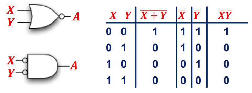
\(A=\overline{(X+Y)}=\overline X \space\overline Y\)
Field-by-field Comparison
| Field | Before | After |
|---|---|---|
| Front | How can we build NOR from NOT and AND? | |
| Back | NOR is equivalent to AND with inputs complemented.<br><br>\(A=\overline{(X+Y)}=\overline X \space\overline Y\)<br><br><img src="paste-4f2a2ce8e54cf095a8c32b10eb76d836070ebd30.jpg"> |
Note 78: ETH::2. Semester::DDCA
Deck: ETH::2. Semester::DDCA
Note Type: Horvath Cloze
GUID:
added
Note Type: Horvath Cloze
GUID:
lSt^W77c/I
Previous
Note did not exist
New Note
Front
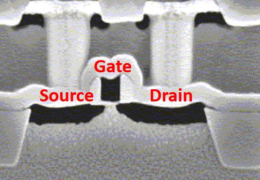
By combining:
- Conductors (Metal)
- Insulators (Oxide)
- Semiconductors
We get a Transistor (MOS).
Back
By combining:
- Conductors (Metal)
- Insulators (Oxide)
- Semiconductors
We get a Transistor (MOS).
Field-by-field Comparison
| Field | Before | After |
|---|---|---|
| Text | <div><strong>By combining:</strong></div> <ol><li>{{c1::Conductors (<b>M</b>etal)}}<br></li> <li>{{c2::Insulators (<strong>O</strong>xide)}}<br></li> <li>{{c3::<strong>S</strong>emiconductors}}<br></li></ol> <div><strong>We get a </strong>{{c4::Transistor (MOS)}}.</div> | |
| Extra | <img src="paste-f9e68afc631519419a56d36751cdb4d5779e1ac1.jpg"> |
Note 79: ETH::2. Semester::DDCA
Deck: ETH::2. Semester::DDCA
Note Type: Horvath Classic
GUID:
added
Note Type: Horvath Classic
GUID:
m6MCp)pX:Q
Previous
Note did not exist
New Note
Front
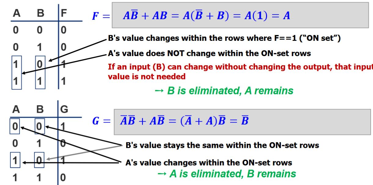
What is the Uniting Theorem?
Back
What is the Uniting Theorem?
\(F=A\overline B+AB\)
Field-by-field Comparison
| Field | Before | After |
|---|---|---|
| Front | What is the Uniting Theorem? | |
| Back | \(F=A\overline B+AB\)<br><br><img src="paste-544b792a3b0a0008ec05e73f83984d8d6b36adab.jpg"> |
Note 80: ETH::2. Semester::DDCA
Deck: ETH::2. Semester::DDCA
Note Type: Horvath Classic
GUID:
added
Note Type: Horvath Classic
GUID:
m7qIFy%!oi
Previous
Note did not exist
New Note
Front
What is a minterm?
Back
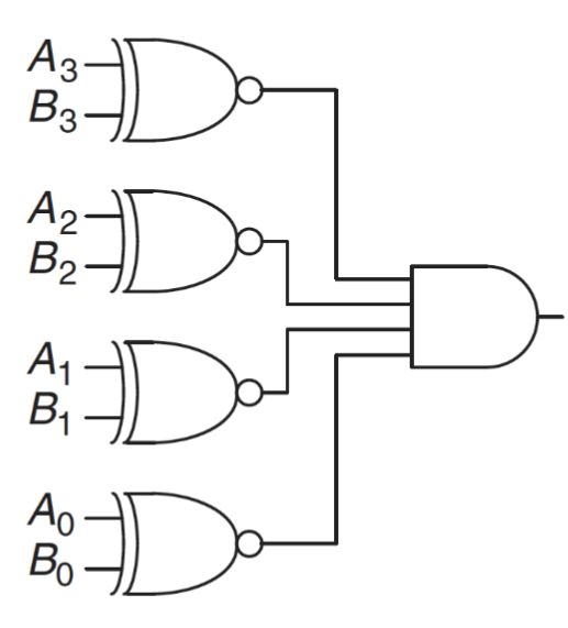
What is a minterm?
A product (AND) that includes all input variables.
\((A \cdot B \cdot \overline{C}) \text{ , } (\overline{A} \cdot \overline{B} \cdot C) \text{ , } (\overline{A} \cdot B \cdot \overline{C})\)
\((A \cdot B \cdot \overline{C}) \text{ , } (\overline{A} \cdot \overline{B} \cdot C) \text{ , } (\overline{A} \cdot B \cdot \overline{C})\)
Field-by-field Comparison
| Field | Before | After |
|---|---|---|
| Front | What is a minterm? | |
| Back | A product (AND) that includes all input variables.<br><br>\((A \cdot B \cdot \overline{C}) \text{ , } (\overline{A} \cdot \overline{B} \cdot C) \text{ , } (\overline{A} \cdot B \cdot \overline{C})\) |
Note 81: ETH::2. Semester::DDCA
Deck: ETH::2. Semester::DDCA
Note Type: Horvath Cloze
GUID:
added
Note Type: Horvath Cloze
GUID:
n!oY_a%~!Q
Previous
Note did not exist
New Note
Front
If the gate of the n-type transistor is supplied with zero voltage, the connection between the source and drain is broken (i.e., the circuit is open).
Back
If the gate of the n-type transistor is supplied with zero voltage, the connection between the source and drain is broken (i.e., the circuit is open).
Field-by-field Comparison
| Field | Before | After |
|---|---|---|
| Text | If the gate of the n-type transistor is supplied with {{c1::zero}} voltage, the connection between the source and drain is {{c2::broken (i.e., the circuit is open)}}. |
Note 82: ETH::2. Semester::DDCA
Deck: ETH::2. Semester::DDCA
Note Type: Horvath Cloze
GUID:
added
Note Type: Horvath Cloze
GUID:
nGy?>L{vz*
Previous
Note did not exist
New Note
Front
A 3-LUT can implement any 3-bit input function.
Back
A 3-LUT can implement any 3-bit input function.
(LUT = Lookup Table)
Field-by-field Comparison
| Field | Before | After |
|---|---|---|
| Text | A 3-LUT can implement {{c1::any 3-bit input function}}. | |
| Extra | (LUT = Lookup Table)<br><br><img src="paste-5ef924f9dd1bae5892f2b78cbd64716dc1471cf4.jpg"> |
Note 83: ETH::2. Semester::DDCA
Deck: ETH::2. Semester::DDCA
Note Type: Horvath Classic
GUID:
added
Note Type: Horvath Classic
GUID:
nZ9{K+v5e:
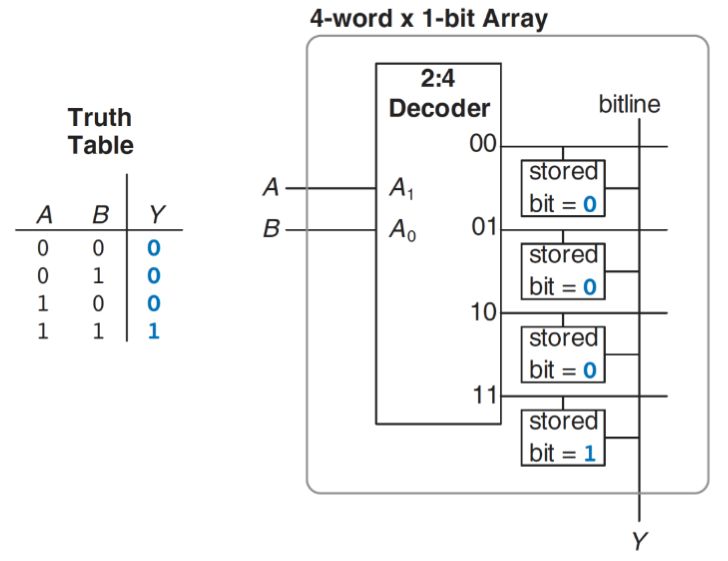
Previous
Note did not exist
New Note
Front
What is this?
Back
What is this?
A state register.
Field-by-field Comparison
| Field | Before | After |
|---|---|---|
| Front | What is this?<br><br><img src="paste-4acc4c494556bcdc7cbaf9afc6e9b6e94385de83.jpg"> | |
| Back | A state register. |
Note 84: ETH::2. Semester::DDCA
Deck: ETH::2. Semester::DDCA
Note Type: Horvath Classic
GUID:
added
Note Type: Horvath Classic
GUID:
nZ:%JyRTd=
Previous
Note did not exist
New Note
Front
What is Addressability?
Back
What is Addressability?
The number of bits of information stored in each location.
E.g. here addressability is 8 bits.
E.g. here addressability is 8 bits.
Field-by-field Comparison
| Field | Before | After |
|---|---|---|
| Front | What is Addressability? | |
| Back | The number of bits of information stored in each location. <br><br>E.g. here addressability is 8 bits.<br><br><img src="paste-cdfafca1398985f93cea204a6b7b7073d008729e.jpg"> |
Note 85: ETH::2. Semester::DDCA
Deck: ETH::2. Semester::DDCA
Note Type: Horvath Cloze
GUID:
added
Note Type: Horvath Cloze
GUID:
n]Q[NPQ}z>
Previous
Note did not exist
New Note
Front
Modern computers use both n-type and p-type transistors, i.e. Complementary MOS (CMOS) technology.
Back
Modern computers use both n-type and p-type transistors, i.e. Complementary MOS (CMOS) technology.
Field-by-field Comparison
| Field | Before | After |
|---|---|---|
| Text | Modern computers use both n-type and p-type transistors, i.e. {{c1::Complementary MOS (CMOS) technology}}. |
Note 86: ETH::2. Semester::DDCA
Deck: ETH::2. Semester::DDCA
Note Type: Horvath Classic
GUID:
added
Note Type: Horvath Classic
GUID:
na4nPYvDI]
Previous
Note did not exist
New Note
Front
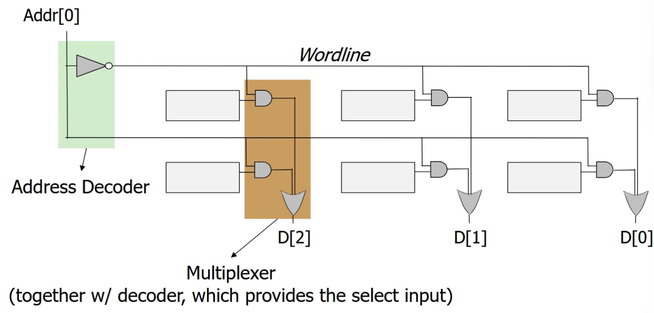
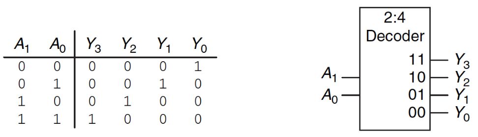
How does a decoder work?
Back
How does a decoder work?
- \(n\) possible inputs and \(2^n\) outputs
- Exactly one of the outputs is 1 and all the rest are 0s
- The output that is logically 1 is the output corresponding to the input pattern that the logic circuit is expected to detect
A decoder is an "input pattern detector".
Example: 2-to-4 decoder
Field-by-field Comparison
| Field | Before | After |
|---|---|---|
| Front | How does a decoder work? | |
| Back | <ol><li>\(n\) possible inputs and \(2^n\) outputs</li><li>Exactly one of the outputs is 1 and all the rest are 0s</li><li>The output that is logically 1 is the output corresponding to the input pattern that the logic circuit is expected to detect</li></ol><div>A decoder is an "input pattern detector".<br></div><div><br></div><div>Example: 2-to-4 decoder</div><div><img src="paste-41f427073aea6bbe436440d617e8ed5e4b95a46e.jpg"><br></div> |
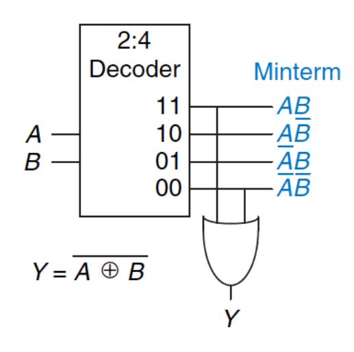
Note 87: ETH::2. Semester::DDCA
Deck: ETH::2. Semester::DDCA
Note Type: Horvath Classic
GUID:
added
Note Type: Horvath Classic
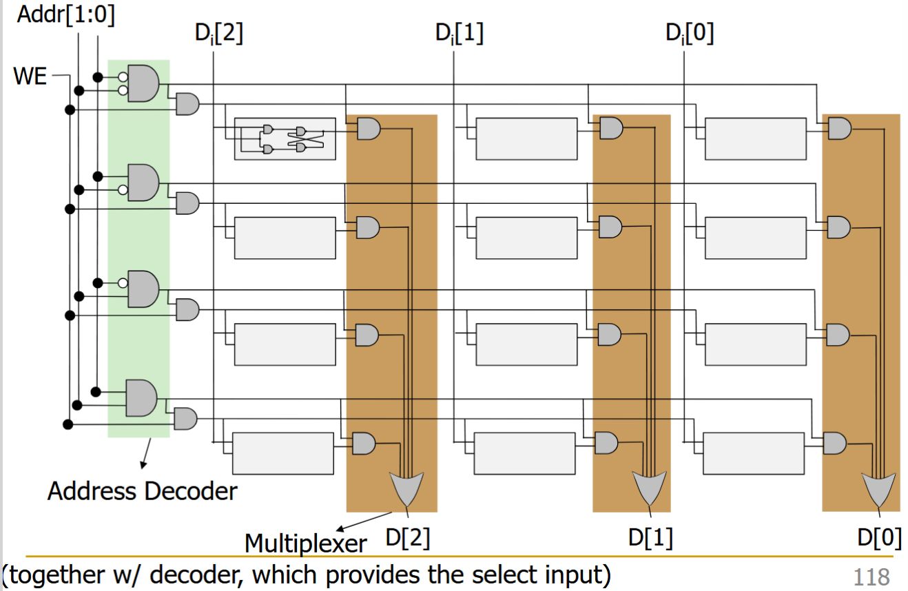
GUID:
o3LWZaHF!=
Previous
Note did not exist
New Note
Front
Writing to Memory
What is \(D_i\) here?
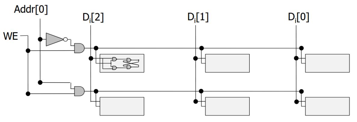
What is \(D_i\) here?
Back
Writing to Memory
What is \(D_i\) here?
What is \(D_i\) here?
Input.
Field-by-field Comparison
| Field | Before | After |
|---|---|---|
| Front | Writing to Memory<br><br>What is \(D_i\) here?<br><br><img src="paste-7e3105fcf0e2a3f5313495e28ac3d165f96c13ac.jpg"> | |
| Back | Input. |
Note 88: ETH::2. Semester::DDCA
Deck: ETH::2. Semester::DDCA
Note Type: Horvath Cloze
GUID:
added
Note Type: Horvath Cloze
GUID:
oFt2FboU]G
Previous
Note did not exist
New Note
Front
\(A\bullet B\) signifies "A and B".
Back
\(A\bullet B\) signifies "A and B".
Field-by-field Comparison
| Field | Before | After |
|---|---|---|
| Text | \(A\bullet B\) signifies {{c1::"A and B"}}. | |
| Extra | <img src="paste-2a88f83499c002bb4aefd9f0fb723e34a306acc2.jpg"><br><img src="paste-5243b849a82a96a61d8a2a0cb57382d5d754be34.jpg"> |
Note 89: ETH::2. Semester::DDCA
Deck: ETH::2. Semester::DDCA
Note Type: Horvath Cloze
GUID:
added
Note Type: Horvath Cloze
GUID:
oJl`_}4^pa
Previous
Note did not exist
New Note
Front
\(X + X \bullet Y = X\)
Back
\(X + X \bullet Y = X\)
Field-by-field Comparison
| Field | Before | After |
|---|---|---|
| Text | \(X + X \bullet Y = {{c1::X}}\) |
Note 90: ETH::2. Semester::DDCA
Deck: ETH::2. Semester::DDCA
Note Type: Horvath Cloze
GUID:
added
Note Type: Horvath Cloze
GUID:
oO*YyBr@a8
Previous
Note did not exist
New Note
Front
We can use D Flip-Flops to implement the state register.
Back
We can use D Flip-Flops to implement the state register.

Field-by-field Comparison
| Field | Before | After |
|---|---|---|
| Text | We can use {{c1::D Flip-Flops}} to implement the state register. | |
| Extra | <img src="paste-2f7dcb7191f560d4f7710228edba5ec2380729ab.jpg"> |
Note 91: ETH::2. Semester::DDCA
Deck: ETH::2. Semester::DDCA
Note Type: Horvath Classic
GUID:
added
Note Type: Horvath Classic
GUID:
oUzmIp%E`>
Previous
Note did not exist
New Note
Front
What's the formula for dynamic power consumption?
Back
What's the formula for dynamic power consumption?
\(C\cdot V^2\cdot f\)
\(C =\) capacitance of the circuit (wires and gates)
\(V =\) supply voltage
\(f =\) charging frequency of the capacitor
\(C =\) capacitance of the circuit (wires and gates)
\(V =\) supply voltage
\(f =\) charging frequency of the capacitor
Field-by-field Comparison
| Field | Before | After |
|---|---|---|
| Front | What's the formula for dynamic power consumption? | |
| Back | \(C\cdot V^2\cdot f\)<br><br>\(C =\) capacitance of the circuit (wires and gates)<br>\(V =\) supply voltage<br>\(f =\) charging frequency of the capacitor |
Note 92: ETH::2. Semester::DDCA
Deck: ETH::2. Semester::DDCA
Note Type: Horvath Cloze
GUID:
added
Note Type: Horvath Cloze
GUID:
o`-s)9=Wl[
Previous
Note did not exist
New Note
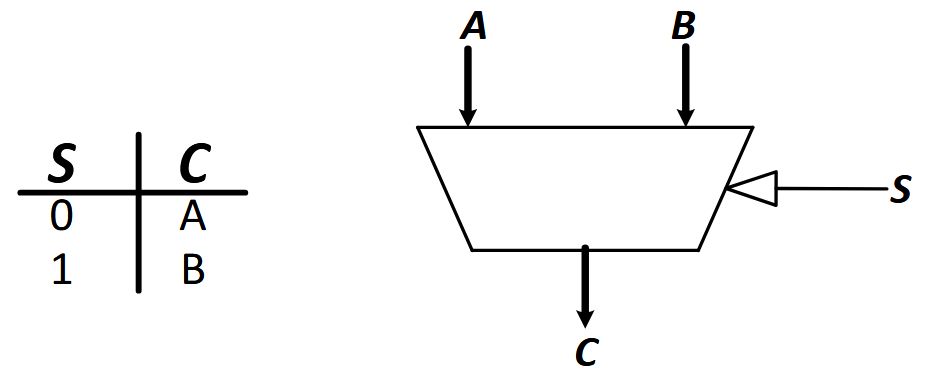
Front
The output C of a MUX is always connected to either the input A or the input B.
Back
The output C of a MUX is always connected to either the input A or the input B.
Output value depends on the value of the select line S.
Field-by-field Comparison
| Field | Before | After |
|---|---|---|
| Text | The output C of a MUX is always connected to {{c1::either the input A or the input B}}. | |
| Extra | Output value depends on the value of the select line S.<br><br><img src="paste-4208651bb851c0f85958e6a1f06734edf09d758c.jpg"> |
Note 93: ETH::2. Semester::DDCA
Deck: ETH::2. Semester::DDCA
Note Type: Horvath Classic
GUID:
added
Note Type: Horvath Classic
GUID:
p2iMO-L)D:
Previous
Note did not exist
New Note
Front
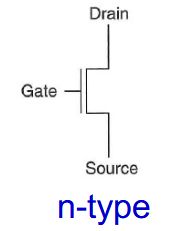
Which type of MOS transistor is this?
Back
Which type of MOS transistor is this?
p-type
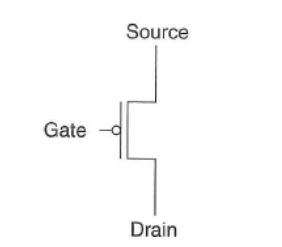
Field-by-field Comparison
| Field | Before | After |
|---|---|---|
| Front | Which type of MOS transistor is this?<br><br><img src="paste-c2def2ad64ef59d3bc9ea12d95969214b321c975.jpg"> | |
| Back | p-type |
Note 94: ETH::2. Semester::DDCA
Deck: ETH::2. Semester::DDCA
Note Type: Horvath Cloze
GUID:
added
Note Type: Horvath Cloze
GUID:
p8m/.jeCY9
Previous
Note did not exist
New Note
Front
When transistors are in series, the network is ON only if all transistors are ON.
Back
When transistors are in series, the network is ON only if all transistors are ON.
Field-by-field Comparison
| Field | Before | After |
|---|---|---|
| Text | When transistors are in series, the network is ON only if {{c1::all transistors are ON}}. |
Note 95: ETH::2. Semester::DDCA
Deck: ETH::2. Semester::DDCA
Note Type: Horvath Cloze
GUID:
added
Note Type: Horvath Cloze
GUID:
pJ5WeT=%X,
Previous
Note did not exist
New Note
Front
Functional specification describes the relationship between inputs and outputs.
Back
Functional specification describes the relationship between inputs and outputs.
Field-by-field Comparison
| Field | Before | After |
|---|---|---|
| Text | Functional specification describes {{c1::the relationship between inputs and outputs}}. |
Note 96: ETH::2. Semester::DDCA
Deck: ETH::2. Semester::DDCA
Note Type: Horvath Classic
GUID:
added
Note Type: Horvath Classic
GUID:
padK$?kSq8
Previous
Note did not exist
New Note
Front
How do we implement a logic function in a PLA?
Back
How do we implement a logic function in a PLA?
Connect the output of an AND gate to the input of an OR gate if the corresponding minterm is included in the SOP.
This is a simple programmable logic construct.
This is a simple programmable logic construct.
Field-by-field Comparison
| Field | Before | After |
|---|---|---|
| Front | How do we implement a logic function in a PLA? | |
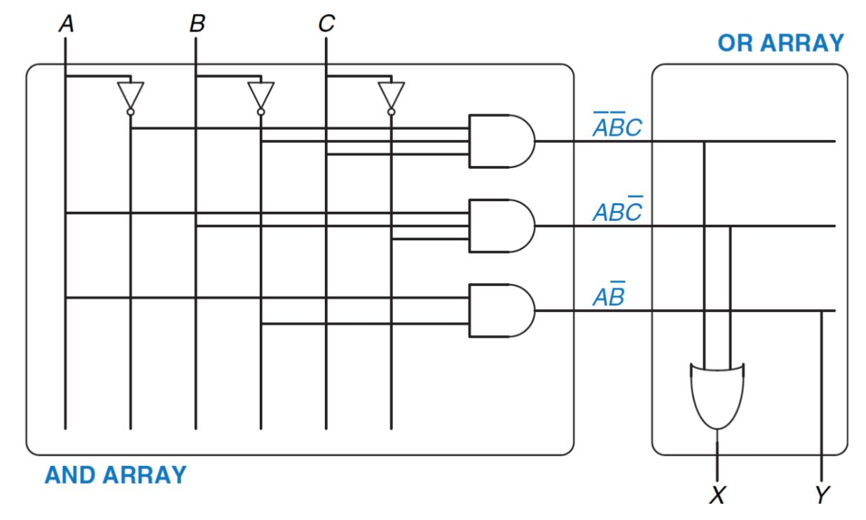
| Back | Connect the output of an AND gate to the input of an OR gate if the corresponding minterm is included in the SOP.<br><br>This is a simple programmable logic construct.<br><br><img src="paste-2fbd7177ca3914ec569c4d1587320498ff0c8fa1.jpg"> |
Note 97: ETH::2. Semester::DDCA
Deck: ETH::2. Semester::DDCA
Note Type: Horvath Cloze
GUID:
added
Note Type: Horvath Cloze
GUID:
p}!>Qc
Previous
Note did not exist
New Note
Front
A FPGA is a software-reconfigurable hardware substrate.
Back
A FPGA is a software-reconfigurable hardware substrate.
- Reconfigurable functions
- Reconfigurable interconnection of functions
- Reconfigurable input/output (IO)
Field-by-field Comparison
| Field | Before | After |
|---|---|---|
| Text | A FPGA is a {{c1::software-reconfigurable hardware substrate}}. | |
| Extra | <ul><li>Reconfigurable functions</li><li>Reconfigurable interconnection of functions</li><li>Reconfigurable input/output (IO)</li></ul> |
Note 98: ETH::2. Semester::DDCA
Deck: ETH::2. Semester::DDCA
Note Type: Horvath Cloze
GUID:
added
Note Type: Horvath Cloze
GUID:
q)+B1jCKdJ
Previous
Note did not exist
New Note
Front
Timing specification describes the delay between inputs changing and outputs responding.
Back
Timing specification describes the delay between inputs changing and outputs responding.
Field-by-field Comparison
| Field | Before | After |
|---|---|---|
| Text | Timing specification describes {{c1::the delay between inputs changing and outputs responding}}. |
Note 99: ETH::2. Semester::DDCA
Deck: ETH::2. Semester::DDCA
Note Type: Horvath Cloze
GUID:
added
Note Type: Horvath Cloze
GUID:
q)njawwNYM
Previous
Note did not exist
New Note
Front
A tri-state buffer enables gating of different signals onto a wire.
Back
A tri-state buffer enables gating of different signals onto a wire.
It acts like a switch.
Field-by-field Comparison
| Field | Before | After |
|---|---|---|
| Text | A tri-state buffer enables {{c1::gating of different signals onto a wire}}. | |
| Extra | <img src="paste-6aad4a37bc003259212e2f00d56e604b0cf5c2b8.jpg"><br><br>It acts like a switch. |
Note 100: ETH::2. Semester::DDCA
Deck: ETH::2. Semester::DDCA
Note Type: Horvath Cloze
GUID:
added
Note Type: Horvath Cloze
GUID:
q,=4BpC=Eo
Previous
Note did not exist
New Note
Front
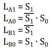
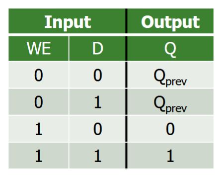
R-S Latch
- Data is stored at Q (inverse at Q')
- S and R are control inputs
- In quiescent (idle) state, both S and R are held at 1
- S (set): drive S to 0 (keeping R at 1) to change Q to 1
- R (reset): drive R to 0 (keeping S at 1) to change Q to 0
Back
R-S Latch
- Data is stored at Q (inverse at Q')
- S and R are control inputs
- In quiescent (idle) state, both S and R are held at 1
- S (set): drive S to 0 (keeping R at 1) to change Q to 1
- R (reset): drive R to 0 (keeping S at 1) to change Q to 0
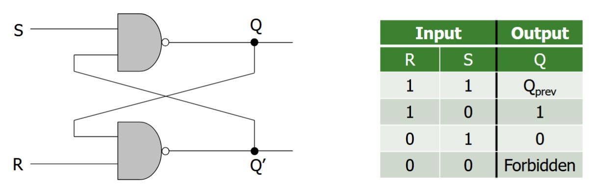
S and R should not both be 0 at the same time.
Field-by-field Comparison
| Field | Before | After |
|---|---|---|
| Text | R-S Latch<br><ul><li>Data is stored at {{c1::Q (inverse at Q')}}</li><li>S and R are {{c2::control inputs}}</li><ul> <li>In quiescent (idle) state, {{c3::both S and R are held at 1}}</li><li>S (set): {{c4::drive S to 0 (keeping R at 1) to change Q to 1}}</li><li>R (reset): {{c4::drive R to 0 (keeping S at 1) to change Q to 0}}</li></ul></ul> | |
| Extra | <img src="paste-d484990009a33988ad2d3a060d667ec92928c41c.jpg"><br><br>S and R should not both be 0 at the same time. |
Note 101: ETH::2. Semester::DDCA
Deck: ETH::2. Semester::DDCA
Note Type: Horvath Classic
GUID:
added
Note Type: Horvath Classic
GUID:
q1yvsXE,ua
Previous
Note did not exist
New Note
Front
Which gate is this?
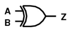
Back
Which gate is this?
XOR
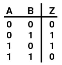
Field-by-field Comparison
| Field | Before | After |
|---|---|---|
| Front | Which gate is this?<br><br><img src="paste-7d4535880d22382faf2a469bb62f36d71ac1ecd9.jpg"> | |
| Back | XOR<br><br><img src="paste-fbcccd66f0a26a44febf8dcce68a686e6461715e.jpg"> |
Note 102: ETH::2. Semester::DDCA
Deck: ETH::2. Semester::DDCA
Note Type: Horvath Cloze
GUID:
added
Note Type: Horvath Cloze
GUID:
qks
Previous
Note did not exist
New Note
Front
The set of gates {AND, OR, NOT} is logically complete because we can build a circuit to carry out the specification of any truth table we wish, without using any other kind of gate.
Back
The set of gates {AND, OR, NOT} is logically complete because we can build a circuit to carry out the specification of any truth table we wish, without using any other kind of gate.
Field-by-field Comparison
| Field | Before | After |
|---|---|---|
| Text | The set of gates {AND, OR, NOT} is {{c1::logically complete}} because we can build a circuit to carry out the specification of any truth table we wish, without using any other kind of gate. |
Note 103: ETH::2. Semester::DDCA
Deck: ETH::2. Semester::DDCA
Note Type: Horvath Cloze
GUID:
added
Note Type: Horvath Cloze
GUID:
qq
Previous
Note did not exist
New Note
Front
\(\overline A\) signifies "not A".
Back
\(\overline A\) signifies "not A".
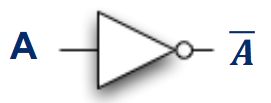
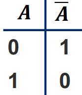
Field-by-field Comparison
| Field | Before | After |
|---|---|---|
| Text | \(\overline A\) signifies {{c1::"not A"}}. | |
| Extra | <img src="paste-d885cebb297fd9ce2e11b004403626df910ecefb.jpg"><br><img src="paste-276f415400a598a88e43cf6a665f2766498f5ec1.jpg"> |
Note 104: ETH::2. Semester::DDCA
Deck: ETH::2. Semester::DDCA
Note Type: Horvath Cloze
GUID:
added
Note Type: Horvath Cloze
GUID:
rJHb8Hi/z_
Previous
Note did not exist
New Note
Front
Sum of Products Form is equivalent to DNF/minterm expansion.
Back
Sum of Products Form is equivalent to DNF/minterm expansion.
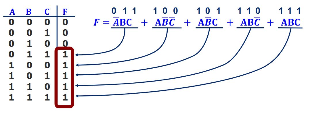
Field-by-field Comparison
| Field | Before | After |
|---|---|---|
| Text | Sum of Products Form is equivalent to {{c1::DNF/minterm expansion}}. | |
| Extra | <img src="paste-49bc2215747c5b28dbf9a8675f61e9ebdb61648d.jpg"> |
Note 105: ETH::2. Semester::DDCA
Deck: ETH::2. Semester::DDCA
Note Type: Horvath Classic
GUID:
added
Note Type: Horvath Classic
GUID:
rKhGk@]2@!
Previous
Note did not exist
New Note
Front
What is dynamic power consumption?
Back
What is dynamic power consumption?
Power used to charge capacitance as signals change (0\(\iff\)1).
Field-by-field Comparison
| Field | Before | After |
|---|---|---|
| Front | What is dynamic power consumption? | |
| Back | Power used to charge capacitance as signals change (0\(\iff\)1). |
Note 106: ETH::2. Semester::DDCA
Deck: ETH::2. Semester::DDCA
Note Type: Horvath Cloze
GUID:
added
Note Type: Horvath Cloze
GUID:
rUfqRU)=~O
Previous
Note did not exist
New Note
Front
\((X + \overline{Y}) \bullet Y = X \bullet Y\)
Back
\((X + \overline{Y}) \bullet Y = X \bullet Y\)
Field-by-field Comparison
| Field | Before | After |
|---|---|---|
| Text | \((X + \overline{Y}) \bullet Y ={{c1:: X \bullet Y}}\) |
Note 107: ETH::2. Semester::DDCA
Deck: ETH::2. Semester::DDCA
Note Type: Horvath Cloze
GUID:
added
Note Type: Horvath Cloze
GUID:
rnH{-|yj$G
Previous
Note did not exist
New Note
Front
A clock synchronizes state changes across many sequential circuit elements.
Back
A clock synchronizes state changes across many sequential circuit elements.
Field-by-field Comparison
| Field | Before | After |
|---|---|---|
| Text | A clock {{c1::synchronizes state changes}} across many sequential circuit elements. |
Note 108: ETH::2. Semester::DDCA
Deck: ETH::2. Semester::DDCA
Note Type: Horvath Classic
GUID:
added
Note Type: Horvath Classic
GUID:
rpAXFA;B;z
Previous
Note did not exist
New Note
Front
What are the two types of MOS transistors?
Back
What are the two types of MOS transistors?
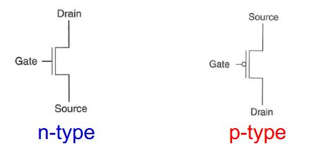
Field-by-field Comparison
| Field | Before | After |
|---|---|---|
| Front | What are the two types of MOS transistors? | |
| Back | <img src="paste-38750c04faf9612e70d859133acd28c824b5e12a.jpg"> |
Note 109: ETH::2. Semester::DDCA
Deck: ETH::2. Semester::DDCA
Note Type: Horvath Classic
GUID:
added
Note Type: Horvath Classic
GUID:
r|D(YkEEE$
Previous
Note did not exist
New Note
Front
What is a maxterm?
Back
What is a maxterm?
A sum (OR) that includes all input variables.
\((A + \overline{B} + \overline{C}) \text{ , } (\overline{A} + B + \overline{C}) \text{ , } (A + B + \overline{C})\)
\((A + \overline{B} + \overline{C}) \text{ , } (\overline{A} + B + \overline{C}) \text{ , } (A + B + \overline{C})\)
Field-by-field Comparison
| Field | Before | After |
|---|---|---|
| Front | What is a maxterm? | |
| Back | A sum (OR) that includes all input variables.<br><br>\((A + \overline{B} + \overline{C}) \text{ , } (\overline{A} + B + \overline{C}) \text{ , } (A + B + \overline{C})\) |
Note 110: ETH::2. Semester::DDCA
Deck: ETH::2. Semester::DDCA
Note Type: Horvath Classic
GUID:
added
Note Type: Horvath Classic
GUID:
r}x`DbeK*8
Previous
Note did not exist
New Note
Front
What are the two main building blocks of FPGAs?
Back
What are the two main building blocks of FPGAs?
Look-Up Tables (LUT) and Switches.
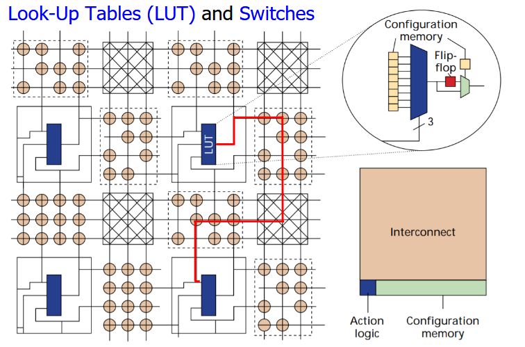
Field-by-field Comparison
| Field | Before | After |
|---|---|---|
| Front | What are the two main building blocks of FPGAs? | |
| Back | Look-Up Tables (LUT) and Switches.<br><br><img src="paste-cee6c807e9f899a8a1405b26996492bb8e767dc2.jpg"> |
Note 111: ETH::2. Semester::DDCA
Deck: ETH::2. Semester::DDCA
Note Type: Horvath Classic
GUID:
added
Note Type: Horvath Classic
GUID:
s&4,le+tM#
Previous
Note did not exist
New Note
Front
What is the non-greyed out part of the circuit?
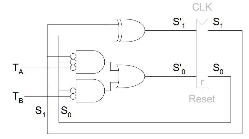
Back
What is the non-greyed out part of the circuit?
Inputs and next state logic.
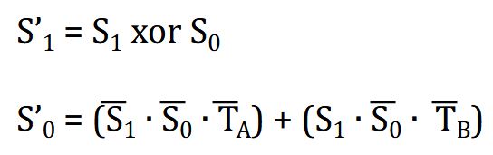
Field-by-field Comparison
| Field | Before | After |
|---|---|---|
| Front | What is the non-greyed out part of the circuit?<br><br><img src="paste-85e71c9bf7ed1a2185c5aced59218c7ccf5c67e2.jpg"> | |
| Back | Inputs and next state logic.<br><br><img src="paste-b7f3dd92498680d0dc3a9552c5869110b8305375.jpg"> |
Note 112: ETH::2. Semester::DDCA
Deck: ETH::2. Semester::DDCA
Note Type: Horvath Cloze
GUID:
added
Note Type: Horvath Cloze
GUID:
s>dpZ2?aZt
Previous
Note did not exist
New Note
Front
Memory is comprised of locations that can be written to or read from.
Back
Memory is comprised of locations that can be written to or read from.
Field-by-field Comparison
| Field | Before | After |
|---|---|---|
| Text | {{c1::Memory}} is comprised of locations that can be written to or read from. |
Note 113: ETH::2. Semester::DDCA
Deck: ETH::2. Semester::DDCA
Note Type: Horvath Cloze
GUID:
added
Note Type: Horvath Cloze
GUID:
sKY>s3R]!/
Previous
Note did not exist
New Note
Front
n-type transistors are good at pulling down the voltage.
Back
n-type transistors are good at pulling down the voltage.
Field-by-field Comparison
| Field | Before | After |
|---|---|---|
| Text | <b>n</b>-type transistors are good at pulling {{c1::dow<b>n</b>}} the voltage. |
Note 114: ETH::2. Semester::DDCA
Deck: ETH::2. Semester::DDCA
Note Type: Horvath Classic
GUID:
added
Note Type: Horvath Classic
GUID:
sQP[*On3|~
Previous
Note did not exist
New Note
Front
Which types of circuits are the three parts of a FSM?
Back
Which types of circuits are the three parts of a FSM?
Sequential Circuits: State register(s)
Combinatorial Circuits: Next state logic, Output logic
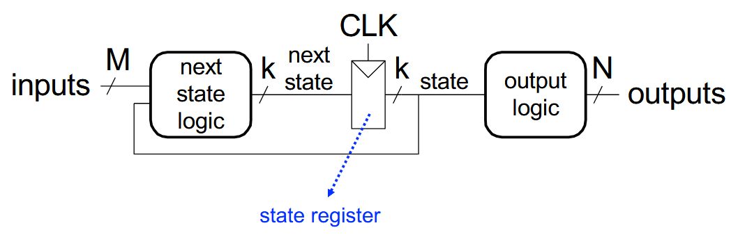
Combinatorial Circuits: Next state logic, Output logic
Field-by-field Comparison
| Field | Before | After |
|---|---|---|
| Front | Which types of circuits are the three parts of a FSM? | |
| Back | Sequential Circuits: State register(s)<br>Combinatorial Circuits: Next state logic, Output logic<br><br><img src="paste-e4af3b21078ddee189e7c5399eb242bb5d90fd10.jpg"> |
Note 115: ETH::2. Semester::DDCA
Deck: ETH::2. Semester::DDCA
Note Type: Horvath Cloze
GUID:
added
Note Type: Horvath Cloze
GUID:
sbwM<`YNbS
Previous
Note did not exist
New Note
Front
To get from voltages to binary values, we can:
- Interpret 0V as logical (binary) 0 value
- Interpret 3V as logical (binary) 1 value
Back
To get from voltages to binary values, we can:
- Interpret 0V as logical (binary) 0 value
- Interpret 3V as logical (binary) 1 value
In the case of the CMOS NOT Gate we then get:
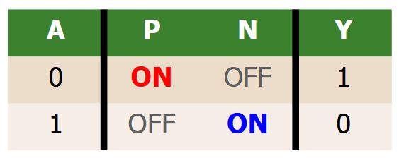
Field-by-field Comparison
| Field | Before | After |
|---|---|---|
| Text | To get from voltages to binary values, we can:<br><ol><li>{{c1::Interpret 0V as logical (binary) 0 value}}</li><li>{{c2::Interpret 3V as logical (binary) 1 value}}</li></ol> | |
| Extra | In the case of the CMOS NOT Gate we then get:<br><br><img src="paste-8bcf6f5a5119256afed57796735aa3578f88b21e.jpg"><br><img src="paste-1ea8562646d826a66676f32131724f1287dda84a.jpg"> |
Note 116: ETH::2. Semester::DDCA
Deck: ETH::2. Semester::DDCA
Note Type: Horvath Cloze
GUID:
added
Note Type: Horvath Cloze
GUID:
sc1PEC3C0X
Previous
Note did not exist
New Note
Front
The entire set of unique locations in memory is referred to as the address space.
Back
The entire set of unique locations in memory is referred to as the address space.
Field-by-field Comparison
| Field | Before | After |
|---|---|---|
| Text | The entire set of unique locations in memory is referred to as {{c1::the address space}}. |
Note 117: ETH::2. Semester::DDCA
Deck: ETH::2. Semester::DDCA
Note Type: Horvath Cloze
GUID:
added
Note Type: Horvath Cloze
GUID:
sdsi1t>JHJ
Previous
Note did not exist
New Note
Front
A clock cycle should be chosen to accommodate the maximum combinational circuit delay.
Back
A clock cycle should be chosen to accommodate the maximum combinational circuit delay.
Field-by-field Comparison
| Field | Before | After |
|---|---|---|
| Text | A clock cycle should be chosen to accommodate {{c1::the maximum combinational circuit delay}}. |
Note 118: ETH::2. Semester::DDCA
Deck: ETH::2. Semester::DDCA
Note Type: Horvath Classic
GUID:
added
Note Type: Horvath Classic
GUID:
spIlS+D;j=
Previous
Note did not exist
New Note
Front
Why is \(R=S=0\) illegal in a R-S Latch?
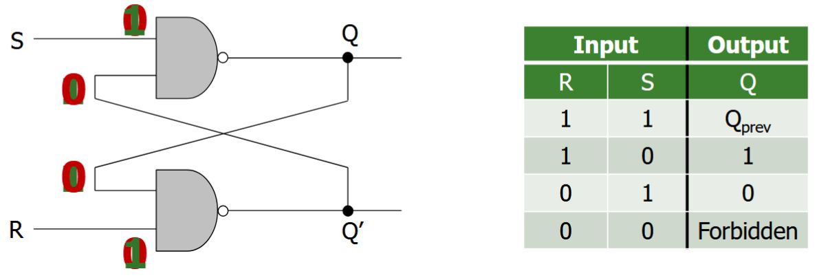
Back
Why is \(R=S=0\) illegal in a R-S Latch?
If \(R=S=0\), \(Q\) and \(Q'\) will both settle to 1, which breaks our invariant that \(Q \neq Q'\).
If \(S\) and \(R\) transition back to 1 at the same time, \(Q\) and \(Q'\) begin to oscillate between 1 and 0 because their final values depend on each other (metastability).
This eventually settles depending on variation in the circuits (more on this in the Timing Lecture).
Field-by-field Comparison
| Field | Before | After |
|---|---|---|
| Front | Why is \(R=S=0\) illegal in a R-S Latch?<br><br><img src="paste-e939b3a4513b1cd81fee9957735bc8b234d94d58.jpg"> | |
| Back | <div>If \(R=S=0\), \(Q\) and \(Q'\) will both settle to 1, which <b>breaks</b> our invariant that \(Q \neq Q'\).</div><div><strong><br></strong></div> <div>If \(S\) and \(R\) transition back to 1 at the same time, \(Q\) and \(Q'\) begin to oscillate between 1 and 0 because their final values depend on each other (<strong>metastability</strong>).</div><div><br></div><div>This eventually settles depending on <strong>variation in the circuits</strong> (more on this in the <strong>Timing Lecture</strong>).</div> |
Note 119: ETH::2. Semester::DDCA
Deck: ETH::2. Semester::DDCA
Note Type: Horvath Classic
GUID:
added
Note Type: Horvath Classic
GUID:
tB@;-gL*Hb
Previous
Note did not exist
New Note
Front
What is this?
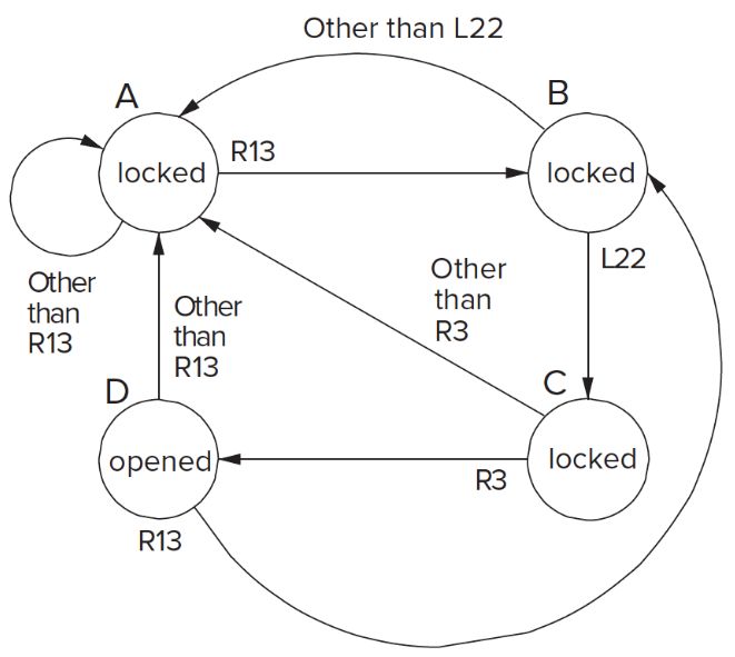
Back
What is this?
State diagram of a sequential lock.
Field-by-field Comparison
| Field | Before | After |
|---|---|---|
| Front | What is this?<br><br><img src="paste-8aec0ef28faf022ade42db3b79a541216adc891c.jpg"> | |
| Back | State diagram of a sequential lock. |
Note 120: ETH::2. Semester::DDCA
Deck: ETH::2. Semester::DDCA
Note Type: Horvath Classic
GUID:
added
Note Type: Horvath Classic
GUID:
tP[&0m}1Mi
Previous
Note did not exist
New Note
Front
What's the critical rule for the networks in a CMOS Gate?

Back
What's the critical rule for the networks in a CMOS Gate?
Exactly one network should be ON, and the other network should be OFF at any given time!
- If both networks are ON at the same time, there is a short circuit → likely incorrect operation.
- If both networks are OFF at the same time, the output is floating → undefined.
Field-by-field Comparison
| Field | Before | After |
|---|---|---|
| Front | What's the critical rule for the networks in a CMOS Gate?<br><br><img src="paste-73917895a320d3ecb9ef27c6b1a82a66e418278e.jpg"> | |
| Back | Exactly one network should be ON, and the other network should be OFF at any given time!<br><div><ul><li>If both networks are ON at the same time, there is a <strong>short circuit</strong> → likely incorrect operation.</li><li>If both networks are OFF at the same time, the output is <strong>floating</strong> → undefined.</li></ul></div> |
Note 121: ETH::2. Semester::DDCA
Deck: ETH::2. Semester::DDCA
Note Type: Horvath Cloze
GUID:
added
Note Type: Horvath Cloze
GUID:
tqA%.|md]&
Previous
Note did not exist
New Note
Front
Output Encoding:
- Outputs are directly accessible in the state encoding
- For the traffic light example, since we have 3 outputs (light color), encode state with 3 bits, where each bit represents a color
- Minimizes output logic
- Only works for Moore Machines (output function of state)
Back
Output Encoding:
- Outputs are directly accessible in the state encoding
- For the traffic light example, since we have 3 outputs (light color), encode state with 3 bits, where each bit represents a color
- Minimizes output logic
- Only works for Moore Machines (output function of state)
Example states: 001, 010, 100, 110
- Bit₀ encodes green light output
- Bit₁ encodes yellow light output
- Bit₂ encodes red light output
Field-by-field Comparison
| Field | Before | After |
|---|---|---|
| Text | <div><div>{{c1::Output}} <strong>Encoding:</strong></div> <ul> <li>Outputs are <strong>directly accessible</strong> in the state encoding</li><li>For the traffic light example, since we have <strong>3 outputs</strong> (light color), encode state with <strong>3 bits</strong>, where each bit represents a color</li><li><strong>Minimizes</strong> {{c2::output logic}}</li><li>Only works for Moore Machines (output function of state)</li></ul></div><br> | |
| Extra | <em>Example states:</em> 001, 010, 100, 110<br><ul><li>Bit₀ encodes <strong>green</strong> light output</li><li>Bit₁ encodes <strong>yellow</strong> light output</li><li>Bit₂ encodes <strong>red</strong> light output</li></ul> |
Note 122: ETH::2. Semester::DDCA
Deck: ETH::2. Semester::DDCA
Note Type: Horvath Cloze
GUID:
added
Note Type: Horvath Cloze
GUID:
u_>,$|fP)p
Previous
Note did not exist
New Note
Front
Binary Encoding (Full Encoding):
- Use the minimum possible number of bits
- Use log₂(num_states) bits to represent the states
- Use log₂(num_states) bits to represent the states
- Minimizes # flip-flops, but not necessarily output logic or next state logic
Back
Binary Encoding (Full Encoding):
- Use the minimum possible number of bits
- Use log₂(num_states) bits to represent the states
- Use log₂(num_states) bits to represent the states
- Minimizes # flip-flops, but not necessarily output logic or next state logic
Example state encodings: 00, 01, 10, 11
Field-by-field Comparison
| Field | Before | After |
|---|---|---|
| Text | <div>{{c1::Binary Encoding (Full Encoding)}}<strong>:</strong></div> <ul> <li>Use {{c3::the minimum possible number of}} bits <ul> <li>{{c3::Use <em>log₂(num_states)</em> bits to represent the states}}<br></li></ul></li> <li><strong>Minimizes</strong> {{c2::# flip-flops, but not necessarily output logic or next state logic}}</li></ul> | |
| Extra | <em>Example state encodings:</em> 00, 01, 10, 11 |
Note 123: ETH::2. Semester::DDCA
Deck: ETH::2. Semester::DDCA
Note Type: Horvath Classic
GUID:
added
Note Type: Horvath Classic
GUID:
uw+8DkpUY4
Previous
Note did not exist
New Note
Front
What is this?
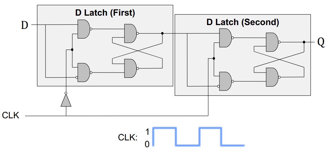
Back
What is this?
A D Flip-Flop.
At the rising edge of clock (clock going from 0\(\rightarrow\)1), Q gets assigned D.
At all other times, Q is unchanged.
At the rising edge of clock (clock going from 0\(\rightarrow\)1), Q gets assigned D.
At all other times, Q is unchanged.
Field-by-field Comparison
| Field | Before | After |
|---|---|---|
| Front | What is this?<br><br><img src="paste-3786bddf98da046a8599b4333c56fc1317667876.jpg"> | |
| Back | A D Flip-Flop.<br><br>At the rising edge of clock (clock going from 0\(\rightarrow\)1), Q gets assigned D.<br>At all other times, Q is unchanged. |
Note 124: ETH::2. Semester::DDCA
Deck: ETH::2. Semester::DDCA
Note Type: Horvath Cloze
GUID:
added
Note Type: Horvath Cloze
GUID:
vK&i;bo$O;
Previous
Note did not exist
New Note
Front
MOS transistors are imperfect switches.
- pMOS transistors pass I's well but 0's poorly (holes carry charge).
- nMOS transistors pass 0's well but I's poorly (electrons carry charge).
Back
MOS transistors are imperfect switches.
- pMOS transistors pass I's well but 0's poorly (holes carry charge).
- nMOS transistors pass 0's well but I's poorly (electrons carry charge).
This is why AND is built with NAND + NOT.
Field-by-field Comparison
| Field | Before | After |
|---|---|---|
| Text | MOS transistors are imperfect switches.<br><ul><li>pMOS transistors pass {{c1::I}}'s well but {{c1::0}}'s poorly {{c1::(holes carry charge)}}.</li><li>nMOS transistors pass {{c1::0}}'s well but {{c1::I}}'s poorly {{c1::(electrons carry charge)}}.</li></ul> | |
| Extra | This is why AND is built with NAND + NOT. |
Note 125: ETH::2. Semester::DDCA
Deck: ETH::2. Semester::DDCA
Note Type: Horvath Classic
GUID:
added
Note Type: Horvath Classic
GUID:
vw*z~aw+{D
Previous
Note did not exist
New Note
Front
Convert this function to canonical form:
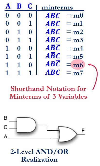
Back
Convert this function to canonical form:
\(\begin{aligned} F(A,B,C) &= \sum m(3,4,5,6,7) \\ &= m3 + m4 + m5 + m6 + m7 \end{aligned}\)
\(F = \overline{A}BC + A\overline{B}\overline{C} + A\overline{B}C + AB\overline{C} + ABC\)
Note that this isn't minimal form! \(\Rightarrow F = A + BC\)
\(F = \overline{A}BC + A\overline{B}\overline{C} + A\overline{B}C + AB\overline{C} + ABC\)
Note that this isn't minimal form! \(\Rightarrow F = A + BC\)
Field-by-field Comparison
| Field | Before | After |
|---|---|---|
| Front | Convert this function to canonical form:<br><br><img src="paste-e22b6a65df1ec4c9f35c5bf2af9104214c84683f.jpg"> | |
| Back | \(\begin{aligned} F(A,B,C) &= \sum m(3,4,5,6,7) \\ &= m3 + m4 + m5 + m6 + m7 \end{aligned}\)<br><br>\(F = \overline{A}BC + A\overline{B}\overline{C} + A\overline{B}C + AB\overline{C} + ABC\)<br><br>Note that this isn't minimal form! \(\Rightarrow F = A + BC\) |
Note 126: ETH::2. Semester::DDCA
Deck: ETH::2. Semester::DDCA
Note Type: Horvath Classic
GUID:
added
Note Type: Horvath Classic
GUID:
v}t`qx*Ktt
Previous
Note did not exist
New Note
Front
How can we use D Latches to implement a FSM?
Back
How can we use D Latches to implement a FSM?
We use a D Flip-Flop
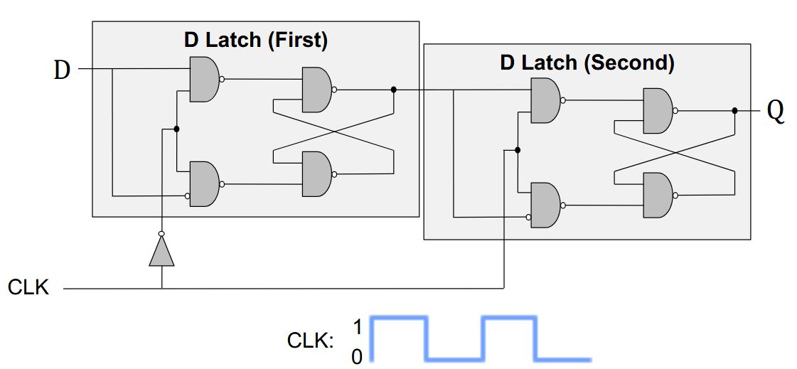
When the clock is low, 1st latch propagates D to the input of the 2nd (Q unchanged).
Only when the clock is high, 2nd latch latches D (Q stores D).
At the rising edge of clock (clock going from 0\(\rightarrow\)1), Q gets assigned D.
When the clock is low, 1st latch propagates D to the input of the 2nd (Q unchanged).
Only when the clock is high, 2nd latch latches D (Q stores D).
At the rising edge of clock (clock going from 0\(\rightarrow\)1), Q gets assigned D.
Field-by-field Comparison
| Field | Before | After |
|---|---|---|
| Front | How can we use D Latches to implement a FSM? | |
| Back | We use a D Flip-Flop<br><img src="paste-cc73c8e859236da274b023d8fb58b5b1d90451f3.jpg"><br><br>When the clock is low, 1st latch propagates D to the input of the 2nd (Q unchanged).<br><br>Only when the clock is high, 2nd latch latches D (Q stores D).<br>At the rising edge of clock (clock going from 0\(\rightarrow\)1), Q gets assigned D. |
Note 127: ETH::2. Semester::DDCA
Deck: ETH::2. Semester::DDCA
Note Type: Horvath Classic
GUID:
added
Note Type: Horvath Classic
GUID:
w&0_XH~|nL
Previous
Note did not exist
New Note
Front
Which gate is this?
Back
Which gate is this?
OR
Field-by-field Comparison
| Field | Before | After |
|---|---|---|
| Front | Which gate is this?<br><br><img src="paste-b40d93ca272769316a76dd3bc8a249b2fae10128.jpg"> | |
| Back | OR<br><br><img src="paste-6e4c2dfe3e807b8506390c3ddfbe974380e318d2.jpg"> |
Note 128: ETH::2. Semester::DDCA
Deck: ETH::2. Semester::DDCA
Note Type: Horvath Classic
GUID:
added
Note Type: Horvath Classic
GUID:
w,kFo*OkK6
Previous
Note did not exist
New Note
Front
What is this?
Back
What is this?
Cross-Coupled Inverters.
Has two stable states: \(Q=1\) or \(Q=0\).
Has a third possible "metastable" state with both outputs oscillating between 0 and 1 (we will see this later).
Not useful without a control mechanism for setting Q.
Has two stable states: \(Q=1\) or \(Q=0\).
Has a third possible "metastable" state with both outputs oscillating between 0 and 1 (we will see this later).
Not useful without a control mechanism for setting Q.
Field-by-field Comparison
| Field | Before | After |
|---|---|---|
| Front | What is this?<br><br><img src="paste-efd9c52b653ff9b4a9524a61121fca9066d0842e.jpg"> | |
| Back | Cross-Coupled Inverters.<br><br>Has two stable states: \(Q=1\) or \(Q=0\).<br>Has a third possible "metastable" state with both outputs oscillating between 0 and 1 (we will see this later).<br><br>Not useful without a <b>control mechanism </b>for setting Q.<br><br><img src="paste-40fef199fe312874c26dd3080f9b553c5504e4ee.jpg"> |
Note 129: ETH::2. Semester::DDCA
Deck: ETH::2. Semester::DDCA
Note Type: Horvath Classic
GUID:
added
Note Type: Horvath Classic
GUID:
w0Wk-s@q$K
Previous
Note did not exist
New Note
Front
What does an ALU do?
Back
What does an ALU do?
It combines a variety of arithmetic and logical operations into a single unit (that performs only one function at a time).
Field-by-field Comparison
| Field | Before | After |
|---|---|---|
| Front | What does an ALU do? | |
| Back | It combines a variety of arithmetic and logical operations into a single unit (that performs only one function at a time).<br><br><img src="paste-d4c76084858a27a2bc15385a19ee00e24b7fc095.jpg"> |
Note 130: ETH::2. Semester::DDCA
Deck: ETH::2. Semester::DDCA
Note Type: Horvath Cloze
GUID:
added
Note Type: Horvath Cloze
GUID:
wK&dW+a*q9
Previous
Note did not exist
New Note
Front
NAND and NOR are logically complete.
Back
NAND and NOR are logically complete.
Field-by-field Comparison
| Field | Before | After |
|---|---|---|
| Text | NAND and NOR are {{c1::logically complete}}. |
Note 131: ETH::2. Semester::DDCA
Deck: ETH::2. Semester::DDCA
Note Type: Horvath Classic
GUID:
added
Note Type: Horvath Classic
GUID:
wfjJW35xJe
Previous
Note did not exist
New Note
Front
Which gate is this?
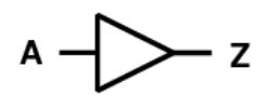
Back
Which gate is this?
Buffer
Field-by-field Comparison
| Field | Before | After |
|---|---|---|
| Front | Which gate is this?<br><br><img src="paste-ec6272f8168e59f9e10c0a00d75245c19c05bf8d.jpg"> | |
| Back | Buffer<br><br><img src="paste-a84f4ec12787c4f030593835d9c2ce773bf394d6.jpg"> |
Note 132: ETH::2. Semester::DDCA
Deck: ETH::2. Semester::DDCA
Note Type: Horvath Cloze
GUID:
added
Note Type: Horvath Cloze
GUID:
x!EU,iyr5{
Previous
Note did not exist
New Note
Front
A FSM consists of these elements:
- A finite number of states
- A finite number of external inputs
- A finite number of external outputs
- An explicit specification of all state transitions
- An explicit specification of what determines each external output value
Back
A FSM consists of these elements:
- A finite number of states
- A finite number of external inputs
- A finite number of external outputs
- An explicit specification of all state transitions
- An explicit specification of what determines each external output value
State: snapshot of all relevant elements of the system at the time of the snapshot
Field-by-field Comparison
| Field | Before | After |
|---|---|---|
| Text | A FSM consists of these elements:<br><ol><li>{{c1::A finite number of states}}</li><li>{{c2::A finite number of external inputs}}<br></li><li>{{c2::A finite number of external outputs}}</li><li>{{c3::An explicit specification of all state transitions}}</li><li>{{c4::An explicit specification of what determines each external output value}}<br></li></ol> | |
| Extra | State: snapshot of all relevant elements of the system at the time of the snapshot |
Note 133: ETH::2. Semester::DDCA
Deck: ETH::2. Semester::DDCA
Note Type: Horvath Classic
GUID:
added
Note Type: Horvath Classic
GUID:
x,YN;U)u48
Previous
Note did not exist
New Note
Front
What's the formula for static power consumption?
Back
What's the formula for static power consumption?
\(V\cdot I_\text{leakage}\)
(supply voltage * leakage current)
(supply voltage * leakage current)
Field-by-field Comparison
| Field | Before | After |
|---|---|---|
| Front | What's the formula for static power consumption? | |
| Back | \(V\cdot I_\text{leakage}\)<br><br>(supply voltage * leakage current) |
Note 134: ETH::2. Semester::DDCA
Deck: ETH::2. Semester::DDCA
Note Type: Horvath Cloze
GUID:
added
Note Type: Horvath Cloze
GUID:
xJUzR))XQ)
Previous
Note did not exist
New Note
Front
When transistors are in parallel, the network is ON if one of the transistors is ON.
Back
When transistors are in parallel, the network is ON if one of the transistors is ON.
Field-by-field Comparison
| Field | Before | After |
|---|---|---|
| Text | When transistors are in parallel, the network is ON if {{c1::one of the transistors is ON}}. |
Note 135: ETH::2. Semester::DDCA
Deck: ETH::2. Semester::DDCA
Note Type: Horvath Occlusio
GUID:
added
Note Type: Horvath Occlusio
GUID:
y!>GF#oDFU
Previous
Note did not exist
New Note
Front
Determine the SOP of \(L_{A1}\) from this output table:
Back
Determine the SOP of \(L_{A1}\) from this output table:
Field-by-field Comparison
| Field | Before | After |
|---|---|---|
| Occlusion | {{c1::image-occlusion:rect:left=.1448:top=.7889:width=.1955:height=.0794:oi=1}}<br> | |
| Image | <img src="paste-2104652c4307f2325008cef16a8a906d2b837817.jpg"> | |
| Header | Determine the SOP of \(L_{A1}\) from this output table: |
Note 136: ETH::2. Semester::DDCA
Deck: ETH::2. Semester::DDCA
Note Type: Horvath Cloze
GUID:
added
Note Type: Horvath Cloze
GUID:
y$t0Kq)TQh
Previous
Note did not exist
New Note
Front
The decoder is useful in determining how to interpret a bit pattern.
Back
The decoder is useful in determining how to interpret a bit pattern.
Field-by-field Comparison
| Field | Before | After |
|---|---|---|
| Text | The {{c1::decoder}} is useful in determining how to interpret a bit pattern. | |
| Extra | <img src="paste-1ce8f7a9f880338a7d797182beb4be144fe192e6.jpg"> |
Note 137: ETH::2. Semester::DDCA
Deck: ETH::2. Semester::DDCA
Note Type: Horvath Classic
GUID:
added
Note Type: Horvath Classic
GUID:
y2>qnHc%Pf
Previous
Note did not exist
New Note
Front
Why can't we simply wire a clock to WE of a D Latch to implement a FSM?
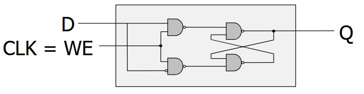
Back
Why can't we simply wire a clock to WE of a D Latch to implement a FSM?
Whenever the clock is high, the latch propagates D to Q.
The latch is "transparent".
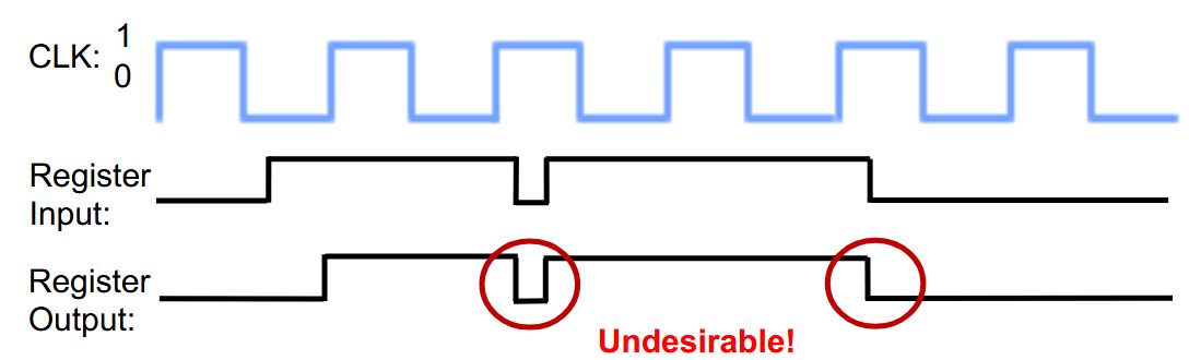
The latch is "transparent".
Field-by-field Comparison
| Field | Before | After |
|---|---|---|
| Front | Why can't we simply wire a clock to WE of a D Latch to implement a FSM?<br><br><img src="paste-efb7af3e85cc5c79a9c81bbd59733d3e8ab3a4d2.jpg"> | |
| Back | Whenever the clock is high, the latch propagates D to Q.<br>The latch is "transparent".<br><br><img src="paste-4414073a5709ca8e5710a64953abd1a4140c689c.jpg"> |
Note 138: ETH::2. Semester::DDCA
Deck: ETH::2. Semester::DDCA
Note Type: Horvath Occlusio
GUID:
added
Note Type: Horvath Occlusio
GUID:
y6L!`3rg+h
Previous
Note did not exist
New Note
Front
What's the difference between these two?

Back
What's the difference between these two?
Field-by-field Comparison
| Field | Before | After |
|---|---|---|
| Occlusion | {{c1::image-occlusion:rect:left=.0066:top=.7908:width=.9822:height=.1903}}<br> | |
| Image | <img src="paste-56ccd7a0fecaeb262dc5922a407d2ee8a4c16d37.jpg"> | |
| Header | What's the difference between these two? |
Note 139: ETH::2. Semester::DDCA
Deck: ETH::2. Semester::DDCA
Note Type: Horvath Cloze
GUID:
added
Note Type: Horvath Cloze
GUID:
yixUKU?m~)
Previous
Note did not exist
New Note
Front
Essence of Simplification (Uniting Theorem)
Find two-element subsets of the ON-set where only one variable changes its value. This single varying variable can be eliminated!
Find two-element subsets of the ON-set where only one variable changes its value. This single varying variable can be eliminated!
Back
Essence of Simplification (Uniting Theorem)
Find two-element subsets of the ON-set where only one variable changes its value. This single varying variable can be eliminated!
Find two-element subsets of the ON-set where only one variable changes its value. This single varying variable can be eliminated!
Field-by-field Comparison
| Field | Before | After |
|---|---|---|
| Text | Essence of Simplification (Uniting Theorem)<br><br>Find two-element subsets of the ON-set where only one variable changes its value. This single varying variable can be {{c1::eliminated}}! |
Note 140: ETH::2. Semester::DDCA
Deck: ETH::2. Semester::DDCA
Note Type: Horvath Cloze
GUID:
added
Note Type: Horvath Cloze
GUID:
zh6Oh%kTi<
Previous
Note did not exist
New Note
Front
How does a rising-clock-edge triggered Flip-Flop work?
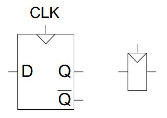
Two inputs: CLK, D
Function:
Two inputs: CLK, D
Function:
- The flip-flop "samples" D on the rising edge of CLK (positive edge)
- When CLK rises from 0 to 1, D passes through to Q
- Otherwise, Q holds its previous value
- Q changes only on the rising edge of CLK
Back
How does a rising-clock-edge triggered Flip-Flop work?
Two inputs: CLK, D
Function:
Two inputs: CLK, D
Function:
- The flip-flop "samples" D on the rising edge of CLK (positive edge)
- When CLK rises from 0 to 1, D passes through to Q
- Otherwise, Q holds its previous value
- Q changes only on the rising edge of CLK
Field-by-field Comparison
| Field | Before | After |
|---|---|---|
| Text | How does a rising-clock-edge triggered Flip-Flop work?<br><br><img src="paste-967b8524a938dc72302521297e9b9c8e8f17928c.jpg"><br><br>Two inputs: CLK, D<br><br>Function:<br><ol><li>The flip-flop "samples" D on {{c1::the rising edge of CLK (positive edge)}}</li><li>When CLK rises from 0 to 1, D {{c2::passes through to Q}}</li><li>Otherwise, {{c2::Q holds its previous value}}</li><li>Q changes only on {{c3::the rising edge of CLK}}</li></ol> |
Note 141: ETH::2. Semester::DDCA
Deck: ETH::2. Semester::DDCA
Note Type: Horvath Classic
GUID:
added
Note Type: Horvath Classic
GUID:
{Na1}u5VN
Previous
Note did not exist
New Note
Front
How can we convert from Minterm to Maxterm?
Back
How can we convert from Minterm to Maxterm?
- Rewrite minterm shorthand using maxterm shorthand
- Replace minterm indices with the indices not already used
Field-by-field Comparison
| Field | Before | After |
|---|---|---|
| Front | How can we convert from Minterm to Maxterm? | |
| Back | <ol><li>Rewrite minterm shorthand using maxterm shorthand</li><li>Replace minterm indices with the indices not already used</li></ol>E.g., \(F(A,B,C) = \sum m(3,4,5,6,7) = \prod M(0,1,2)\) |